Last Minute Notes Computer Organization
Last Updated :
07 Mar, 2024
Basic Terminology
- Control Unit – A control unit (CU) handles all processor control signals. It directs all input and output flow, fetches the code for instructions and controlling how data moves around the system.
- Arithmetic and Logic Unit (ALU) – The arithmetic logic unit is that part of the CPU that handles all the calculations the CPU may need, e.g. Addition, Subtraction, Comparisons. It performs Logical Operations, Bit Shifting Operations, and Arithmetic Operation.
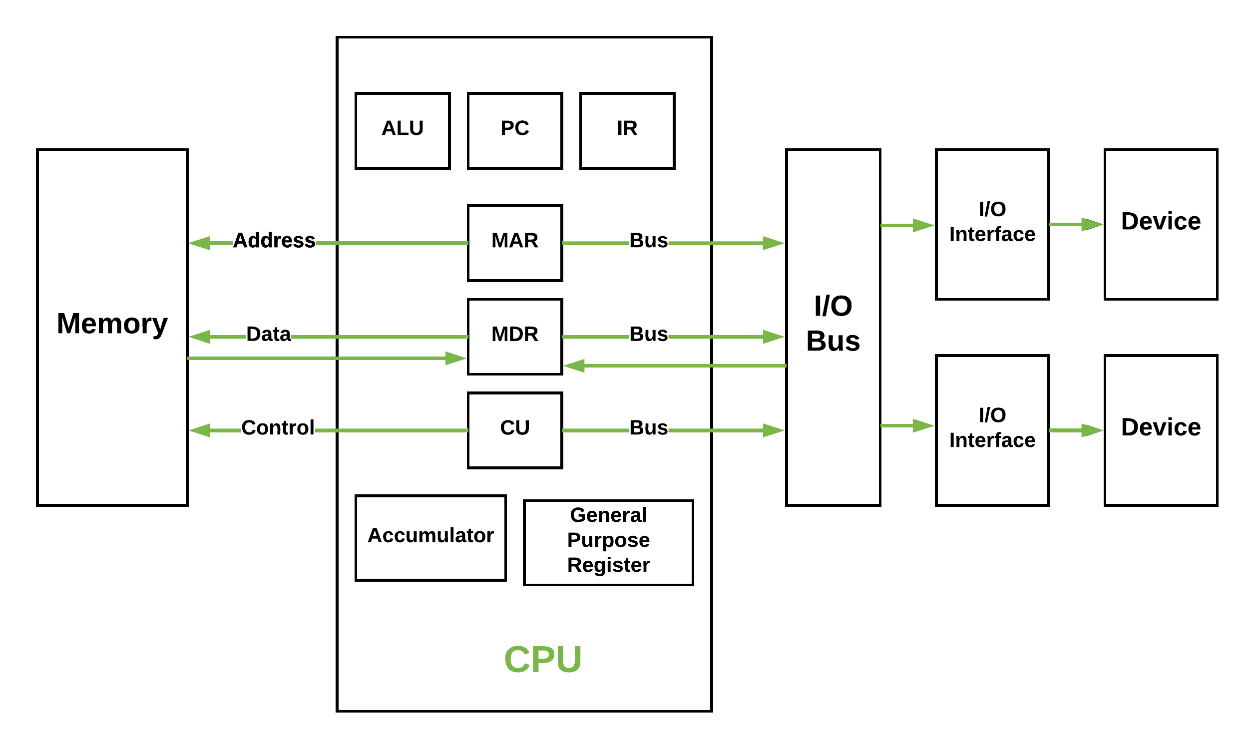 Figure – Basic CPU structure, illustrating ALU
 - Main Memory Unit (Registers) –
- Accumulator: Stores the results of calculations made by ALU.
- Program Counter (PC): Keeps track of the memory location of the next instructions to be dealt with. The PC then passes this next address to Memory Address Register (MAR).
- Memory Address Register (MAR): It stores the memory locations of instructions that need to be fetched from memory or stored into memory.
- Memory Data Register (MDR): It stores instructions fetched from memory or any data that is to be transferred to, and stored in, memory.
- Current Instruction Register (CIR): It stores the most recently fetched instructions while it is waiting to be coded and executed.
- Instruction Buffer Register (IBR): The instruction that is not to be executed immediately is placed in the instruction buffer register IBR.
- Input/Output Devices – Program or data is read into main memory from the input device or secondary storage under the control of CPU input instruction. Output devices are used to output the information from a computer.
- Buses – Data is transmitted from one part of a computer to another, connecting all major internal components to the CPU and memory, by the means of Buses. Types:
- Data Bus: It carries data among the memory unit, the I/O devices, and the processor.
- Address Bus: It carries the address of data (not the actual data) between memory and processor.
- Control Bus: It carries control commands from the CPU (and status signals from other devices) in order to control and coordinate all the activities within the computer.
A instruction is of various length depending upon the number of addresses it contain. Generally CPU organization are of three types on the basis of number of address fields:
- Single Accumulator organization
- General register organization
- Stack organization
- Zero Address Instructions – Address is stored in the opcode, in the zero address instruction. A stack based organization uses zero address instruction.
- One Address Instructions – This use a implied ACCUMULATOR register for data manipulation. One operand is in accumulator and other is in register or memory location. Implied means that the CPU already know that one operand is in accumulator so there is no need to specify it. i.e there will be one opcode field and one address field.
- Two Address Instructions – Here two address can be specified in the instruction. Unlike earlier in one address instruction, the result was stored in accumulator here result can be stored at a different location rather than just accumulator, but require the number more of the bit to represent address.
- Three Address Instructions – This has three address field to specify a register or a memory location. The program created is much short in size but the number of bits per instruction increase.
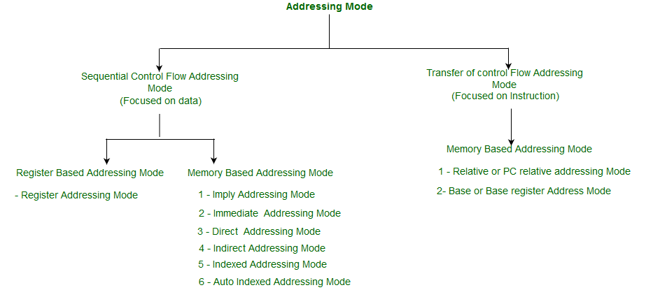
The term addressing modes refers to the way in which the operand of an instruction is specified. The addressing mode specifies a rule for interpreting or modifying the address field of the instruction before the operand is actually executed. An assembly language program instruction consists of two parts

IMPORTANT TERMS
- Starting address of memory segment.
- Effective address or Offset: An offset is determined by adding any combination of three address elements: displacement, base and index.
- Displacement: It is an 8 bit or 16 bit immediate value given in the instruction.
- Base: Contents of base register, BX or BP.
- Index: Content of index register SI or DI.
- Implied mode:: In implied addressing the operand is specified in the instruction itself. In this mode the data is 8 bits or 16 bits long and data is the part of instruction.Zero address instruction are designed with implied addressing mode.
- Immediate addressing mode (symbol #):In this mode data is present in address field of instruction .Designed like one address instruction format. Note:Limitation in the immediate mode is that the range of constants are restricted by size of address field.
- Register mode: In register addressing the operand is placed in one of 8 bit or 16 bit general purpose registers. The data is in the register that is specified by the instruction. Here one register reference is required to access the data.
- Register Indirect mode: In this addressing the operand’s offset is placed in any one of the registers BX, BP, SI, DI as specified in the instruction. The effective address of the data is in the base register or an index register that is specified by the instruction. Here two register reference is required to access the data.
- Auto Indexed (increment mode): Effective address of the operand is the contents of a register specified in the instruction. After accessing the operand, the contents of this register are automatically incremented to point to the next consecutive memory location.(R1)+. Here one register reference, one memory reference, and one ALU operation is required to access the data.
- Auto indexed ( decrement mode): Effective address of the operand is the contents of a register specified in the instruction. Before accessing the operand, the contents of this register are automatically decremented to point to the previous consecutive memory location. –(R1)Here one register reference, one memory reference and one ALU operation is required to access the data.
- Auto decrement mode is the same as the auto-increment mode. Both can also be used to implement a stack as push and pop. Auto increment and Auto-decrement modes are useful for implementing “Last-In-First-Out” data structures.
- Direct addressing/ Absolute addressing Mode (symbol [ ]): The operand’s offset is given in the instruction as an 8 bit or 16 bit displacement element. In this addressing mode, the 16-bit effective address of the data is part of the instruction. Here only one memory reference operation is required to access the data.
- Indirect addressing Mode (symbol @ or () ):In this mode address field of instruction contains the address of effective address.Here two references are required. 1st reference to get an effective address. 2nd reference to access the data.
- Indexed addressing mode: The operand’s offset is the sum of the content of an index register SI or DI and an 8 bit or 16-bit displacement.
- Based Indexed Addressing: The operand’s offset is sum of the content of a base register BX or BP and an index register SI or DI.
- Based on Transfer of control, addressing modes are:
- Characteristic of RISC –
- Simpler instruction, hence simple instruction decoding.
- Instruction come under size of one word.
- Instruction take single clock cycle to get executed.
- More number of general purpose register.
- Simple Addressing Modes.
- Less Data types.
- Pipelining can be achieved.
- Characteristic of CISC –
- Complex instruction, hence complex instruction decoding.
- Instruction are larger than one word size.
- Instruction may take more than single clock cycle to get executed.
- Less number of general purpose register as operation get performed in memory itself.
- Complex Addressing Modes.
- More Data types.
- Hardwired Control Unit –
- Fixed logic circuits that correspond directly to the Boolean expressions are used to generate the control signals.
- Hardwired control is faster than micro-programmed control.
- A controller that uses this approach can operate at high speed.
- RISC architecture is based on hardwired control unit.
- Micro-programmed Control Unit –
- The control signals associated with operations are stored in special memory units inaccessible by the programmer as Control Words.
- Control signals are generated by a program are similar to machine language programs.
- Micro-programmed control unit is slower in speed because of the time it takes to fetch microinstructions from the control memory.
- There are two type Micro-programmed control Unit:
- Horizontal Micro-programmed control Unit- The control signals are represented in the decoded binary format that is 1 bit/CS.
- Vertical Micro-programmed control Unit – The control signals re represented in the encoded binary format. For N control signals- Logn(N) bits are required.
- Registers Involved In Each Instruction Cycle:
- Memory address registers(MAR) : It is connected to the address lines of the system bus. It specifies the address in memory for a read or write operation.
- Memory Buffer Register(MBR) : It is connected to the data lines of the system bus. It contains the value to be stored in memory or the last value read from the memory.
- Program Counter(PC) : Holds the address of the next instruction to be fetched.
- Instruction Register(IR) : Holds the last instruction fetched.

- The
- Indirect Cycle
- is always followed by the
- Execute Cycle
- . The
- Interrupt Cycle
- is always followed by the
- Fetch Cycle
- . For both fetch and execute cycles, the next cycle depends on the state of the system.
- The Fetch Cycle – At the beginning of the fetch cycle, the address of the next instruction to be executed is in the Program Counter(PC).
- The Indirect Cycles – Once an instruction is fetched, the next step is to fetch source operands. Source Operand is being fetched by indirect addressing it can be fetched by any addressing mode, here its done by indirect addressing). Register-based operands need not be fetched. Once the opcode is executed, a similar process may be needed to store the result in the main memory.
- The Execute Cycle The other three cycles(Fetch, Indirect and Interrupt) are simple and predictable. Each of them requires a simple, small and fixed sequence of micro-operations. In each case, the same micro-operation is repeated each time around. Execute Cycle is different from them. Like, for a machine with N different opcodes there are N different sequences of micro-operations that can occur.
- The Interrupt Cycle: At the completion of the Execute Cycle, a test is made to determine whether any enabled interrupt has occurred or not. If an enabled interrupt has occurred then Interrupt Cycle occurs. The nature of this cycle varies greatly from one machine to another.
- Microprogram:
- Program stored in memory that generates all control signals required to execute the instruction set correctly, it consists micro-instructions.
- Micro-instruction:
- Contains a sequencing word and a control word. The control word is all control information required for one clock cycle.
- Micro-operations:
- Micro-operations are the atomic operations which executes a particular micro-instruction. Example of micro-operation during the fetch cycle:
t1: MAR ←(PC)
t2: MBR ←Memory
PC ←(PC) + I
t3: IR ←(MBR)
Memory Organization :
- Memories are made up of registers. Each register in the memory is one storage location. The storage location is also called a memory location. Memory locations are identified using Address. The total number of bit a memory can store is its capacity.
| Byte Addressable Memory | Word Addressable Memory |
|---|
| When the data space in the cell = 8 bits then the corresponding address space is called as Byte Address. | When the data space in the cell = word length of CPU then the corresponding address space is called as Word Address. |
| Based on this data storage i.e. Bytewise storage, the memory chip configuration is named as Byte Addressable Memory. | Based on this data storage i.e. Wordwise storage, the memory chip configuration is named as Word Addressable Memory. |
- Simultaneous access memory organization:
- If H1 and H2 are the Hit Ratios and T1 and T2 are the access time of L1 and L2 memory levels respectively then the
- Average Memory Access Time
- can be calculated as:
- [Tex]T=(H1*T1)+((1-H1)*H2*T2[/Tex]
- Hierarchical Access Memory Organizations:
- If H1 and H2 are the Hit Ratios and T1 and T2 are the access time of L1 and L2 memory levels respectively then the
- Average Memory Access Time
- can be calculated as:
- [Tex]T=(H1*T1)+((1-H1)*H2*(T1+T2)[/Tex]
- Cache Memory is a special very high-speed memory. It is used to speed up and synchronizing with high-speed CPU. Levels of memory: Level 1 or Register, Level 2 or Cache memory, Level 3 or Main Memory, Level 4 or Secondary Memory.
Hit ratio = hit / (hit + miss) = no. of hits/total accesses
- Cache Mapping:
- There are three different types of mapping used for the purpose of cache memory which is as follows: Direct mapping, Associative mapping, and Set-Associative mapping.
- Direct Mapping – Maps each block of main memory into only one possible cache line. If a line is previously taken up by a memory block and a new block needs to be loaded, the old block is trashed. An address space is split into two parts index field and a tag field. The cache is used to store the tag field whereas the rest is stored in the main memory.
- Associative Mapping – A block of main memory can map to any line of the cache that is freely available at that moment. The word offset bits are used to identify which word in the block is needed, all of the remaining bits become Tag.
- Set-Associative Mapping – Cache lines are grouped into sets where each set contains k number of lines and a particular block of main memory can map to only one particular set of the cache. However, within that set, the memory block can map to any freely available cache line.
- Note: Translation Lookaside Buffer (i.e. TLB) is required only if Virtual Memory is used by a processor. In short, TLB speeds up the translation of virtual address to a physical address by storing page-table in faster memory. In fact, TLB also sits between the CPU and Main memory.
- Locality of reference –
- Since size of cache memory is less as compared to main memory. So to check which part of main memory should be given priority and loaded in the cache is decided based on the locality of reference.
- Types of Locality of reference
- Spatial Locality of reference Spatial locality means instruction or data near to the current memory location that is being fetched, may be needed soon in the near future.
- Temporal Locality of reference Temporal locality means current data or instruction that is being fetched may be needed soon. So we should store that data or instruction in the cache memory to avoid searching again in main memory for the same data.
- Write Policy
- Write Through: In this technique, all write operations are made to main memory as well as to the cache, ensuring that main memory is always valid. For hierarchical access: [Tex] T_{read} = H \times T_{cache} + (1-H) \times (T_{cache} + T_{memory\_block}) \newline
= T_{cache} + (1-H) \times T_{memory\_block}[/Tex] For simultaneous access : [Tex]T_{read} = H \times T_{cache} + (1-H) \times (T_{memory\_block})
\newline
T_{write} = T_{memory\_word}
[/Tex]
- Write Back: In write-back updates are made only in the cache. When an update occurs, a dirty bit, or use bit, associated with the line is set. Then, when a block is replaced, it is written back to main memory if and only if the dirty bit is set. For hierarchical access: [Tex] T_{read} = T_{write} = H \times T_{cache} + (1-H) \times (T_{cache} + T_{memory\_block} + T_{write\_back}) \\= T_{cache} + (1-H) \times (T_{memory\_block} + T_{write\_back}), \\ \text{ where } T_{write\_back} = x \times T_{memory\_block}, \text{ where } x \text{ is the fraction of dirty blocks}[/Tex] For simultaneous access : [Tex]T_{read} = T_{write} = H \times T_{cache} + (1-H) \times ( T_{memory\_block} + T_{write\_back}), \\ \text{ where } T_{write\_back} = x \times T_{memory\_block}, \text{ where } x \text{ is the fraction of dirty blocks} [/Tex]
- Pipelining is a process of arrangement of hardware elements of the CPU such that its overall performance is increased. Simultaneous execution of more than one instruction takes place in a pipelined processor. RISC processor has 5 stage instruction pipeline to execute all the instructions in the RISC instruction set. Following are the 5 stages of RISC pipeline with their respective operations:
- Stage 1 (Instruction Fetch) In this stage the CPU reads instructions from the address in the memory whose value is present in the program counter.
- Stage 2 (Instruction Decode) In this stage, instruction is decoded and the register file is accessed to get the values from the registers used in the instruction.
- Stage 3 (Instruction Execute) In this stage, ALU operations are performed.
- Stage 4 (Memory Access) In this stage, memory operands are read and written from/to the memory that is present in the instruction.
- Stage 5 (Write Back) In this stage, computed/fetched value is written back to the register present in the instructions.
- Performance of a pipelined processor
- Consider a ‘k’ segment/stages pipeline with clock cycle time as ‘Tp’. Let there be ‘n’ tasks to be completed in the pipelined processor. So, time taken to execute ‘n’ instructions in a pipelined processor:
ETpipeline = k + n – 1 cycles
= (k + n – 1) Tp
- In the same case, for a non-pipelined processor, execution time of ‘n’ instructions will be:
ETnon-pipeline = n * k * Tp
- So, speedup (S) of the pipelined processor over non-pipelined processor, when ‘n’ tasks are executed on the same processor is:
S = Performance of pipelined processor /
Performance of Non-pipelined processor
- As the performance of a processor is inversely proportional to the execution time, we have,
S = ETnon-pipeline / ETpipeline
=> S = [n * k * Tp] / [(k + n – 1) * Tp]
S = [n * k] / [k + n – 1]
- When the number of tasks ‘n’ are significantly larger than k, that is, n >> k
S = n * k / n
S = k
- where ‘k’ are the number of stages in the pipeline. Also,
- Efficiency
- = Given speed up / Max speed up = S / S
- max
- We know that, Smax = k So,
- Efficiency
- = S / k
- Throughput
- = Number of instructions / Total time to complete the instructions So,
- Throughput
- = n / (k + n – 1) * Tp Note: The cycles per instruction (CPI) value of an ideal pipelined processor is 1
- Performance of pipeline with stalls
- Speed Up (S) = CPI
- non-pipeline
- / (1 + Number of stalls per instruction)
- Dependencies and Data Hazard
- There are mainly three types of dependencies possible in a pipelined processor. These are :
- Structural dependency:
- This dependency arises due to the resource conflict in the pipeline. A resource conflict is a situation when more than one instruction tries to access the same resource in the same cycle. A resource can be a register, memory, or ALU.
- To minimize structural dependency stalls in the pipeline, we use a hardware mechanism called Renaming.
- Control Dependency (Branch Hazards):
- This type of dependency occurs during the transfer of control instructions such as BRANCH, CALL, JMP, etc. On many instruction architectures, the processor will not know the target address of these instructions when it needs to insert the new instruction into the pipeline. Due to this, unwanted instructions are fed to the pipeline.
- Branch Prediction is the method through which stalls due to control dependency can be eliminated. In this at 1st stage prediction is done about which branch will be taken.
- For branch prediction Branch penalty is zero. The number of stalls introduced during the branch operations in the pipelined processor is known as branch penalty.
- Data Dependency (Data Hazard):
- Data hazards occur when instructions that exhibit data dependence, modify data in different stages of a pipeline. Hazard cause delays in the pipeline. There are mainly three types of data hazards: 1) RAW (Read after Write) [Flow/True data dependency] 2) WAR (Write after Read) [Anti-Data dependency] 3) WAW (Write after Write) [Output data dependency]
- To minimize data dependency stalls in the pipeline, operand forwarding is used.
- In operand forwarding, we use the interface registers present between the stages to hold intermediate output so that dependent instruction can access new value from the interface register directly.
- The input/output (I/O) architecture is computer system’s interface to the outside world. Each I/O module interfaces to the system bus and controls one or more peripheral devices.
- There are three basic forms of input and output systems –
- Programmed I/O: In programmed I/O, the processor executes a program that gives its direct control of the I/O operation, including sensing device status, sending a read or write command, and transferring the data.
- Interrupt driven I/O: In interrupt driven I/O, the processor issues an I/O command, continues to execute other instructions, and is interrupted by the I/O module when the I/O module completes its work.
- Direct Memory Access(DMA): In Direct Memory Access (DMA), the I/O module and main memory exchange data directly without processor involvement.
- There are several ways to represent floating point number but IEEE 754 is the most efficient in most cases. IEEE 754 has 3 basic components:
- The Sign of Mantissa – This is as simple as the name. 0 represents a positive number while 1 represents a negative number.
- The Biased exponent – The exponent field needs to represent both positive and negative exponents. A bias is added to the actual exponent in order to get the stored exponent.
- The Normalised Mantisa – The mantissa is part of a number in scientific notation or a floating-point number, consisting of its significant digits. Here we have only 2 digits, i.e. O and 1. So a normalised mantissa is one with only one 1 to the left of the decimal.
| TYPES | SIGN | BIASED EXPONENT | NORMALISED MANTISA | BIAS |
|---|
| Single precision | 1(31st bit) | 8(30-23) | 23(22-0) | 127 |
| Double precision | 1(63rd bit) | 11(62-52) | 52(52-0) | 1023 |
- Formula for finding decimal value:
- Decimal value = (-1)
- s
- * 1.F * 2
- (E-Bias)
- , Where E is decimal value of exponent field, F is mantissa and s is sign bit.
Flag register
- (a) Status Flags
- Zero Flag (Z): When an arithmetic operation results in zero, the flip-flop called the Zero flag – which is set to one.
- Carry flag (CY): After an addition of two numbers, if the sum in the accumulator is larger than eight bits, then the flip-flop uses to indicate a carry called the Carry flag, which is set to one.
- Parity (P): If the result has an even number of 1s, the flag is set to 1; for an odd number of 1s the flag is reset.
- Auxiliary Carry (AC): In an arithmetic operation, when a carry is generated from lower nibble and passed on to higher nibble then this register is set to 1.
- Sign flag(S): It is a single bit in a system status (flag) register used to indicate whether the result of the last mathematical operation resulted in a value in which the most significant bit was set.
- (b) Control Flags
- Trap Flag (TF): It sets to enable one step execution of program. This is used for debug purpose.
- Interrupt Flag (IF): It is used to enable or disable interrupt during execution.
- Direction Flag (DF): The direction flag is a flag that controls the left-to-right or right-to-left direction of string processing.
Share your thoughts in the comments
Please Login to comment...