Digital electronics or digital technology is a branch of engineering that deals with electronics operating on digital signals. Digital circuits are designed using logic gates and the minimization of digital circuits is possible because of simplified logic gate functions and their implementation.
Here, we have covered the top 50 digital electronics interview questions along with their answers. These are frequently asked Digital Electronics Interview Questions.

Digital Electronics Interview Questions
Here are some basic as well as advanced electronics interview questions along with their answers:
1. What are the properties of Boolean Algebra?
Some basic switching properties of Boolean algebra are:
- Annulment law: A.0 = 0 ; A + 1 = 1
- Associative law:A+(B+C) = (A+B)+C ; A.(B.C) = (A.B).C
- Absorption law: A. (A+B) =A ; A+AB = A
- Complement law: A+A’ =1 ; A.A’ = 0
- Commutative law: A+B = B+A; A.B =B.A
- De Morgan Law: (A.B)’ = A’ +B’ ; (A+B)’ = A’.B’
- Distributive law: A. (B+C) = (A.B)+(A.C)
- Double negation law: ((A)’)’ = A
- Identity law: A.1 = A; A + 0 = A
- Idempotent law: A+A =A ; A.A=A
To read more, refer to the article: Properties of boolean algebra
2. Explain the Consensus Theorem.
The consensus theorem is defined as follows in digital electronics:
AB + A'C + BC = AB + A'C
The consensus or resolvent of the terms AB and A’C is BC. It is the intersection of all the unique literals of the terms, excluding the literal that appears negated in one term and unnegated in the other.
To read more, refer to the article: Consensus Theorem
3. What is Gray code?
Gray Code is also known as Reflected Binary code. It is a binary system in which each successive pair of numbers differs with only 1-bit data. These codes are very useful in binary numbers generated by hardware that can produce an error during the transition from one number to another.
To read more, refer to the article: Gray Code
4. Describe Encoder and Decoder.
The encoder and decoder are combinational logic circuits. An encoder is a device that converts analog or active data into digital or coded data. But the decoder’s operation is exactly the reverse of the encoder. A decoder is a device that converts the original signal as output from the coded input signal and converts n lines of input into 2n lines of output.
To read more, refer to the article: Encoder and Decoder
5. Explain the difference between Sequential and Combinational circuits.
| 1. |
The output depends on the present input only and there is no need for feedback for input and output, so a memory element is not required. |
The output depends upon both the present input and the present state (previous output), so a memory element is required to save the feedback state. |
| 2. |
Clock signals are not required and the combinational circuit is not dependent on time. |
Clock signals are required and sequential circuits are dependent on time and clock so it needs triggering. |
| 3. |
It is easier to use, design, and handle. |
It is more complex to use, design, and handle. |
| 4. |
Faster logic circuits. |
Slower than combinational circuits. |
| 5. |
Elementary building blocks are logic gates only. |
Elementary building blocks are Flip-Flops. |
To read more, refer to the article: Sequential vs Combinational circuits
6. What is the difference between Latch And Flip-flop?
| 1 |
Flip-flops are bistable devices i.e., it has two stable states and those states are represented as 0 and 1. |
The latch is also a bistable device and those states are also represented as 0 and 1. |
| 2 |
It is an edge-triggered device. |
It is a level-triggered device. |
| 3 |
It checks the inputs but changes the output only at times defined by the clock signal or any other control signal. |
It checks the inputs continuously and responds to the changes in inputs immediately. |
| 4 |
Flip-flop always has a clock signal. |
The latch doesn’t have a clock signal |
| 5 |
ex:D Flip-flop, JK Flip-flop |
ex: SR Latch, D Latch |
To read more, refer to the article: Latch vs Flip Flop
7. Explain De Morgan’s Theorem.
De Morgan’s Theorem is expressed using the following two theorems:
- The complement of a product of two numbers is the sum of the complements of those numbers.
(A. B)’ = A’ + B’
- The complement of the sum of two numbers is equal to the product of the complement of two numbers.
(A + B)’ = A’B’
To read more, refer to the article: Proof of De Morgan’s Theorem
8. How many types of number systems are there?
A Number system is defined as an elementary system to represent numbers and figures. It is a unique way of expressing numbers in arithmetic and algebraic structure. Based on the base value and the number of allowed digits, number systems are of many types. The four common types of Number systems are:
- Binary Number System.
- Octal Number System.
- Decimal Number System.
- Hexadecimal Number System.
To read more, refer to the article: How many types of number systems are there?
9. What is a Logic gate?
A logic gate is a switching circuit that decides whether an input pulse can pass to the output in digital circuits. Logic gates are the building blocks of a digital circuit, that executes various logical operations required by any digital circuit. It can take two or more inputs but produces only one output.
The combination of inputs applied to a logic gate identifies its output. Logic gates use Boolean algebra expressions to execute logical processes. Logic gates are found in nearly every digital device.
To read more, refer to the article: Logic Gate
10. What are the types of Logic gates?
There are three basic logic gates, two universal gates, and a few other combinational logic gates in digital electronics.
Basic Gates:
- AND gate.
- OR gate.
- NOT gate.
Universal Gates:
Other Gates:
To read more, refer to the article: Types of Logic Gate
11. What is meant by K-Map or Karnaugh Map?
K-map is a table-like representation of a boolean expression. K-map is used to minimize the Boolean expression so that the circuit can be implemented using the least number of gates and become more efficient. K-map is a table-like representation but it gives more information than TRUTH TABLE. Boolean expressions with 3 and 4 variables can be minimized very easily using K-map without using any Boolean algebra theorems, but using K-map for more than 4 variables is a bit complex as it needs two or more K-maps and it cannot apply for more than 6 variable. K-map can be resolved into two forms Sum of Product (SOP) and Product of Sum (POS) as per the need of the problem.
To read more, refer to the article: Introduction of K-Map
12. Difference between SOP and POS?
| 1. |
A way of representing boolean expressions as the sum of product terms. |
A way of representing boolean expressions as a product of sum terms. |
| 2. |
SOP uses minterms. Minterm is a product of boolean variables either in normal form or complemented form. |
POS uses max terms. Maxterm is the sum of boolean variables either in normal form or complemented form. |
| 3. |
SOP is formed by considering all the minterms, whose output is HIGH(1) |
POS is formed by considering all the maxterms, whose output is LOW(0) |
| 4. |
It is the sum of minterms. Minterms are represented as ‘m’ |
It is a product of max terms. Max terms are represented as ‘M’ |
| 5. |
Input with value 1 is assumed as the variable itself and input with value 0 is assumed as a complement of the input. |
Input with value 1 is assumed as the complement, and input with value 0 is assumed as the variable itself. |
To read more, refer to the article: Difference between SOP and POS
13. Write down the Characteristics of Digital ICs.
The characteristics of digital ICs are:
- Propagation delay: It is the average transition time delay for the propagation of a signal.
- Power Dissipation: Total power consumption by the gate when it is completely occupied.
- Fan-in: Number of inputs connected to a circuit without any degradation in the voltage level.
- Fan-out: Number of standard loads carried out by the gate without halting its normal operation.
- Noise Margin: It is the maximum noise added to the input of the circuit so that there is no change in the output.
14. What are the limitations of the Karnaugh Map?
The limitations of the Karnaugh Map are as follows:
- It cannot minimize boolean expressions with seven or more variables. It can map only six variables.
- Useful when expressions are in standard form.
15. What are the advantages of the K-Map Method?
The advantages of the K-Map method are:
- It simplifies and minimizes boolean expressions up to four variables excellently.
- It gives us a visual method for logical simplification.
- Suitable for both SOP and POS forms.
16. Define Pair, Quad, and Octet.
- Pair: Two adjacent cells of the K-map are known as Pair. It cancels or minimizes expression with one variable in a K-Map simplification.
- Quad: Four adjacent pairs in a K-map are known as quads. It cancels or minimizes expression with two variables in a K-Map simplification.
- Octet: Eight adjacent pairs in a K-map are known as octets. It cancels or minimizes expression with four variables in a K-map simplification.
17. Explain the Quine-MC Cluskey method?
The Quine McCluskey method or tabulation method is used to minimize the Boolean functions. This method simplifies boolean expression into the simplified form using prime applicants. This method is convenient to simplify when boolean expressions have more than 4 input variables.
To read more, refer to the article: Quine McCluskey Method
18. Explain the Duality Theorem.
Dual expression is equal to a negative logic of the given boolean relation. For this, we have to,
- Change each OR sign by and AND sign and vice-versa.
- Complement any 0 or 1 appearing in the expression.
- Keep the literal same.
Example:
Dual of A(B+C) = A+(B.C) = (A+B)(A+C)
19. What is Half-Adder?
Half adder is used to perform the addition of 2 bits using a combinational circuit. The input variables are augend and addend bits and the output variables are sum & carry bits.
Truth Table:
To read more, refer to the article: Half Adder
20. What is Full-Adder?
Full Adder adds three inputs and produces two outputs. The first two inputs are A and B and the third input is carried input denoted as C-IN. The output carry is defined as C-OUT and the normal output is defined as S which is SUM.
A full adder logic is designed in such a manner that can take eight inputs together to create a byte-wide adder and cascade the carry bit from one adder to another.
Full Adder Truth Table:
To read more, refer to the article: Full Adder
21. What is a Multiplexer?
The multiplexer is a combinational circuit it has many data inputs and a single output depending on the control/select lines. For N number of input lines, log n (base2) is the total selection lines, or for 2n input lines, the total n number of selection lines is needed.
Multiplexers are also known as “Data n selector, parallel to serial converter, many to one circuit, parallel to serial converter, universal logic circuit”. Multiplexers are basically used to increase the amount of data that can be sent over the network within a specific amount of time and bandwidth.
To read more, refer to the article: Multiplexer in Digital Electronics
22. What are the applications of multiplexers?
The applications of the multiplexer are as follows:
- Used in the time-multiplexing system.
- It is used as an A/D to D/A Converter.
- Used in the data acquisition system
- It is used as a data selector.
23. What is a Demultiplexer?
The demultiplexer is a data distributor that takes a single input and gives multiple outputs. Demultiplexers have 1 input and 2n output lines where n is the selection line.
24. What are the applications of Demultiplexer?
The applications of the demultiplexer are as follows:
- It is used as a decoder for the conversion of binary to decimal.
- It is used as a serial-to-parallel converter.
- Used in the data transmission system for error detection.
25. Define Rise Time, Fall time, Hold time, and Setup time.
- Rise time: Time required to change the voltage level from 10% to 90%.
- Fall time: Time that is required to change the voltage level from 90% to 10%.
- Hold Time: The lowest time at which the voltage level becomes constant after triggering the clock pulse to clock into the flip flop reliably is known as the Hold time. It is denoted by thold.
- Setup time: The minimum time required to maintain the constant voltage levels at the excitation inputs of the flip-flop device before the triggering edge of the clock pulse reliably clocked in the flip-flop is called the Setup time. It is denoted as tsetup.
26. What is the difference between Synchronous and Asynchronous Counters?
| 1. |
All flip-flops are triggered with the same clock simultaneously. |
Different flip-flops are triggered with different clocks, not simultaneously. |
| 2. |
A synchronous Counter is faster than an asynchronous counter in operation. |
The asynchronous Counter is slower than the synchronous counter in operation. |
| 3. |
Also known as Parallel Counter. |
Also known as Serial Counter. |
| 4. |
Examples: Ring counter, Johnson counter. |
Examples: Ripple UP counter and the Ripple DOWN counter. |
| 5. |
In synchronous counter, propagation delay is less. |
In the asynchronous counter, there is a high propagation delay. |
To read more, refer to the article: Differences between Synchronous and Asynchronous Counter
27. What are the Flip-Flops?
Flip-flops are the basic digital memory circuit. It has two states logic 1(High) and logic 0(low) states. A flip-flop is a sequential circuit that consists of a single binary state of information or data. It is also known as a Bistable Multivibrator. Flip-flops are used as the delay element they are also used for Frequency Division, Data transfer, Counting, and as a memory element.
To read more, refer to the article: Flip Flop and its Type
28. Explain One-hot Key Design?
One hot encoding is used in the process of categorizing data variables to be used in machine learning algorithms for making better predictions. In one-hot encoding, we convert each categorical value into a different column, and in return, it gives a binary value, either 0 or 1 to each column. And each integer value represents a binary vector.
To read more, refer to the article: What is One Hot Design?
29. Define CAM?
Content addressable memory (CAM) is a data storage device, that stores memory in cells. When any data is entered into the memory, the CAM compares the input with all the stored data. It is a high-speed technology. In CAM, memories are unsorted, which means they are not arranged in chronological order and are not packed in isolated modules.
To read more, refer to the article: Content addressable memory
30. What are Standard and Canonical forms?
- Standard Form: A Boolean variable that can be represented in either true form or complemented form. In standard form, the Boolean function will contain all the variables in either true form or complemented form while a canonical number of variables depends on the output of SOP or POS.
- Canonical Form: In Boolean algebra, the Boolean function can be expressed as Canonical Disjunctive Normal Form known as minterm and some are expressed as Canonical Conjunctive Normal Form known as maxterm.
In Minterm, we look for the functions where the output results in “1” while in Maxterm we look for functions where the output results in “0”.
We perform the Sum of minterm also known as the Sum of products (SOP).
We perform Product of Maxterm also known as Product of Sum (POS).
Boolean functions expressed as a sum of minterms or product of maxterms are said to be in canonical form.
To read more, refer to the article: Canonical and Standard Form
31. Explain Functional Completeness.
A set of operations is said to be functionally complete or universal if every switching function can be represented by operations in it. In simple words, a set of Boolean functions is functionally complete, if all other Boolean functions can be constructed from this set and a set of input variables are provided, e.g.
- Set B = {+,’} are functionally complete
- Set A = {+,*,’ (OR, AND, complement) } are functionally complete.
- Set C = {*,’} are functionally complete
To read more, refer to the article: Functional Completeness
32. Discuss various implicants in K-Map.
Implicant is defined as a product/minterm term in SOP or sum/maxterm term in POS of a Boolean function. Consider a boolean function, F = AB + ABC + BC. The implicants are AB, ABC, and BC. There are various implicants in the K-Map, which are as follows:
- Prime Implicant: A group of squares or rectangles made up of a bunch of adjacent minterms which is allowed by the definition of K-Map are called prime implicants(PI) i.e. all possible groups formed in K-Map.
- Redundant Prime Implicant: The prime implicants for which each of its minterms is covered by some essential prime implicants are redundant prime implicants(RPI). This prime implicant never appears in the final solution.
- Essential Prime Implicant: These are those subcubes(groups) that cover at least one minterm that can’t be covered by any other prime implicant. Essential prime implicants(EPI) are those prime implicants that always appear in the final solution.
- Selective Prime Implicant: The prime implicants that are neither essential nor redundant prime implicants are called selective prime implicants(SPI) or non-essential prime implicants. They may appear in some solutions or may not appear in some solutions.
To read more, refer to the article: Various Implicants in K-Map
33. What is Hazard?
A hazard, in a digital circuit, causes a transient fluctuation in the output of the circuit. A hazard in a digital circuit is a temporary disruption in the operation of the circuit which resolves itself after some time. These fluctuations happen when different paths from the input to output have delays and this leads to changes in input variables. These do not change the output instantly but appear at the output after a small delay.
There are three different kinds of hazards found in digital circuits:
- Static hazard
- Functional hazard
- Dynamic hazard
34. What is Static Hazard?
A static hazard happens when a change in input causes the output before stabilizing to its correct value. There are two types of static hazards, which are as follows:
- Static-0 Hazard: If the output is currently at logic state 0 and after the input changes its state, the output changes momentarily to 1 before settling on 0, then it is said to be a Static-0 hazard.
- Static-1 Hazard: If the output is currently at logic state 1 and after the input changes its state, the output changes momentarily to 0 before settling on 1, then it is said to be a Static-1 hazard.
35. Define Dynamic Hazard?
When the output changes several times then it should change from 0 to 1 or 1 to 0 only once, it is called a dynamic hazard. Dynamic hazards occur only in multilevel circuits. Dynamic hazards take place when the output changes for two neighbouring input combinations while changing, the output should change only once. But sometimes it may change three or more times in short intervals because of different delays in several paths.
36. Difference between Static and Dynamic Hazards?
| 1 |
Static hazards occur when an input changes and it causes the output to change at the same moment before output becomes stable. |
Dynamic hazards occur when output changes for two adjacent inputs while the output should change only once. |
| 2 |
Occurs in combinational circuits. |
Occurs only in multilevel circuits. |
| 3 |
Easy to resolve. |
Complex to resolve. |
| 4 |
Can be eliminated by using redundant gates. |
Removal of static-1 hazard ensures no occurrence of a dynamic hazard. |
| 5 |
It causes a temporary false output value. |
It results in a transition to the wrong stable state. |
To read more, refer to the article: Static vs Dynamic Hazard
37. Explain the types of Flip Flop.
Flip-flops are the basic digital memory circuit. It has two states logic 1(High) and logic 0(low) states. A flip-flop is a sequential circuit that consists of a single binary state of information or data. It is also known as a Bistable Multivibrator.
Types of flip-flops:
- RS Flip Flop
- JK Flip Flop
- D Flip Flop
- T Flip Flop
To read more, refer to the article: Types of Flip Flop
38. Difference between SR and JK flip flop?
JK Flip Flop: The JK flip-flop’s diagram describes the basic structure which has Clock (CLK), Clear (CLR), and Preset (PR).
Operations in JK Flip-Flop:
PR = CLR = 0
This condition is in an invalid state.
PR = 0 and CLR = 1
The PR is activated, which means the output in the Q is set to 1. So, the flip-flop is in the set state.
PR = 1 and CLR = 0
The CLR is activated which means the output in the Q’ is set to 1. So, the flip-flop is in the reset state.
PR = CLR = 1
In this condition, the flip-flop works in its normal way whereas the PR and CLR get deactivated.
SR Flip Flop: In SR flip flop, with the help of Preset and Clear, when the power is switched ON, the state of the circuit is uncertain and keeps on changing. It may Set (Q = 1) or Reset (Q’ = 0) state. In many applications, it is desired to initially Set or Reset the flip flop. This thing is accomplished by the Preset (PR) and the Clear (CLR).
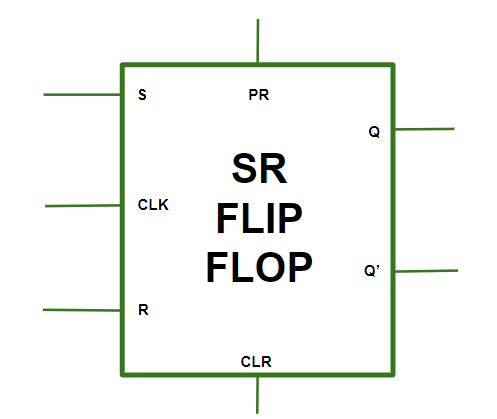
SR Flip FLop
Operations in SR Flip-Flop:
PR = CLR = 1
The asynchronous inputs are inactive and the flip-flop responds independently to the S, R, and CLK inputs.
PR = 0 and CLR = 1
When the Q is set to 1.
PR = 1 and CLR = 0
When the Q’ is set to 1.
PR = CLR = 0
This is an invalid state.
To read more, refer to the article: Difference between SR and JK flip flop
39. Discuss Master-Slave JK flip flop.
The Master-Slave Flip-Flop is a combination of two JK flip-flops linked together in a series manner. One of them acts as the “master” and the other behaves as a “slave”. The output from the master flip flop is linked with the two inputs of the slave flip flop whose output is again feedback to the inputs of the master flip flop.
Other than this, the circuit has an inverter. The inverter is connected to the clock pulse in such a manner that the inverted clock pulse is given to the slave flip-flop. In other words, if the clock pulse equals zero, i.e. CP=0 for a master flip-flop, then the clock pulse equals one, i.e. CP=1 for a slave flip-flop, and if CP=1 for the master flip flop then it becomes 0 for the slave flip-flop.
To read more, refer to the article: Master-Slave JK Flip Flop
40. What is the Basic Bistable element?
A bit memory cell is also called a Basic Bistable element. It has two cross-coupled inverters, and 2 outputs Q and Q’. It is called “Bistable” as the basic bistable element circuit has two stable states logic 0 and logic 1.
The following diagram shows the Basic Bistable element:
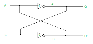
Basic Bistable Element
(A) when A=0,
     In inverter1, Q = A'= B= 1
     In inverter2, Q' = B' = A = 0

(B) when A=1,
     In inverter1, Q = A'= B= 0
     In inverter2, Q' = B' = A = 1
To read more, refer to the article: One-bit memory cell
41. What is a counter?
It is a device that stores (and sometimes displays) the number of times a particular event or process has occurred, often in relationship to a clock signal. Counters are used in digital electronics for counting purposes, they can count specific events happening in the circuit. For example, in the UP counter, a counter increases the count for every rising edge of the clock. Not only counting, but a counter can also follow a certain sequence based on our design like any random sequence 0,1,3,2….They can also be designed with the help of flip-flops.
Counters are broadly divided into two categories:
- Asynchronous counter
- Synchronous counter
To read more, refer to the article: Counters
42. What is Jhonson Counter?
Johnson counters also called creeping counter is a type of synchronous counter. In the Johnson counter, the complemented output of the last flip-flop is linked to the input of the first flip-flop, and for implementing the n-bit Johnson counter we need n number of flip-flops. It is one of the most important types of shift register counter. It originated from the feedback of the output to its own input. Johnson counter is a ring with an inversion. Other names for the Johnson counter are the walking counter, creeping counter, mobile counter, twisted ring counter, and switch tail counter.
To read more, refer to the article: Jhonson Counter
43. A ripple counter can count up to how many states?
A ripple counter can count up to 2n states with n-bits. It is also known as MOD n counter. It is known as a ripple counter because the clock pulse ripples through the flip-flops. Some of the features of the ripple counter are:
- All the flip-flops are used in toggle mode.
- It is an asynchronous counter.
- Only one flip-flop is connected with an external clock pulse and another flip-flop clock is obtained from the output of the previous flip-flop.
- Different flip-flops are used with a different clock pulse.
- The flip-flop applied with an external clock pulse acts as LSB (Least Significant Bit) in the counting sequence.
To read more, refer to the article: Ripple Counter
44. What are shift registers?
A Register is used to store information. A register is a group of flip-flops that are connected in series and used to store multiple bits of data.
The information stored within registers can be transferred with the help of shift registers. Shift Register is also a group of flip-flops that is used to store multiple bits of data. The bits stored in shift registers can be moved within the registers and in/out of the registers by using clock pulses. An n-bit shift register can be obtained by joining n flip-flops.
The registers that will shift the bits to the right are called “Shift right registers”.
The registers that will shift the bits to the left are called “Shift left registers”.
Shift registers are basically of 4 types. These are:
- Parallel In parallel Out shift register
- Parallel In Serial Out shift register
- Serial In Serial Out shift register
- Serial In parallel Out shift register
To read more, refer to the article: Shift Registers
45. Explain Ring Counter?
A ring counter is a typical application of the Shift register. The ring counter is almost the same as the shift counter. The only change is that the output of the last flip-flop is connected to the input of the first flip-flop in the case of the ring counter but in the case of the shift register it is taken as output. Except for this, all the other things are the same.
No. of states in Ring counter = No. of flip-flop used
So, for designing a 4-bit Ring counter we need 4 flip-flops.
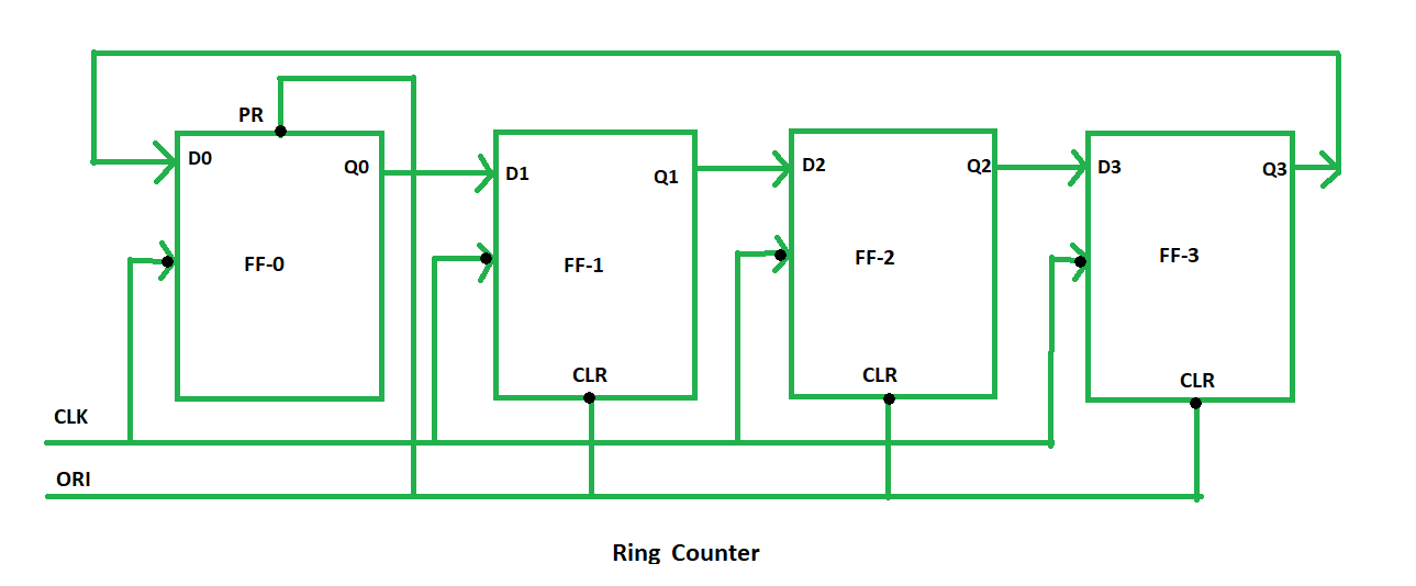
To read more, refer to the article: Ring Counter
46. What is Scrambling?
Scrambling is a technique that does not increase the number of bits and does provide synchronization. The problem with techniques like Bipolar AMI(Alternate Mark Inversion) is that continuous sequences of zeroes create synchronization problems one solution to this is Scrambling.
There are two common scrambling techniques:
- B8ZS(Bipolar with 8-zero substitution)
- HDB3(High-density bipolar3-zero)
To read more, refer to the article: Scrambling
47. Difference between PLA and PAL?
| 1. |
PLA stands for Programmable Logic Array. |
While PAL stands for Programmable Array Logic. |
| 2. |
PLA speed is lower than PAL. |
While PAL’s speed is higher than PLA. |
| 3. |
The complexity of PLA is high. |
While PAL’s complexity is less. |
| 4. |
The cost of PLA is also high. |
While the cost of PAL is low. |
| 5. |
Programmable Logic Array is less available. |
While Programmable Array Logic is more available than Programmable Logic Array. |
| 6. |
It is less used than PAL. |
While it is more used than PLA. |
To read more, refer to the article: Difference between Programmable Logic Array and Programming Array Logic
48. Difference Between Digital And Analog Systems?
Analog and digital signals are used to transmit information (such as audio or video), usually through electric signals. In digital technology, information is translated into binary format (either 0 or 1) and information is translated into electric pulses of varying amplitude in analog technology.
| Signal |
Represents physical measurements. |
They are discrete and generated by digital modulation. |
| Waves |
Sine Waves |
Square Waves |
| Representation |
It uses a continuous range of values to represent information |
Digital system uses discrete values to represent information |
| Technology |
Records waveforms as they are. |
Samples analog waveforms into a limited set of numbers and then records them. |
| Data transmissions |
Affected by noise during transmission and write/read cycle. |
Noise-immune during transmission and write/read cycle. |
49. Explain Operational Amplifier.
An amplifier increases the strength of the input signal. It can be a Current amplifier, whose input is some current and output is amplified current. Voltage amplifiers, whose input is some voltage and output is amplified voltage.
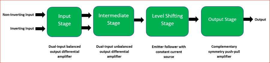
- Transimpedance amplifier, its input is some current and the output is the voltage.
- Transconductance amplifier, its input is some voltage and the output is the current.
To read more, refer to the article: Operational Amplifier
50. Difference between Broadband and broadband transmission?
| 1. |
It is bidirectional in nature. |
It is unidirectional in nature. |
| 2. |
Digital signalling is used. |
Analog signalling is used. |
| 3. |
It works excellently with bus topology. |
It can be used with a bus as well as tree topology. |
| 4. |
Signals can only travel over short distances. |
Signals can be travelled over long distances without being attenuated. |
| 5. |
In baseband transmission, Manchester and Differential Manchester encoding are used. |
Only PSK encoding is used. |
To read more, refer to the article: Difference between Broadband and Baseband Transmission
Final Words
Digital electronics interview questions are designed to assess your knowledge of the fundamental concepts of digital electronics, such as logic gates, Boolean algebra, and digital circuits. The questions may also be specific to the type of digital electronics job that you are applying for.
Digital Electronics Interview Questions – FAQs
1. What is the difference between a latch and a flip-flop?
A latch is a circuit that stores a single bit of data. A flip-flop is a circuit that stores a single bit of data and can also be used to count or sequence signals.
2. What is the binary number system?
The binary number system is a base-2 number system. This means that each digit in a binary number can be either a 0 or a 1.
3. State the De Morgan’s Theorem.
De Morgan’s Theorem states that the complement of the product of two Boolean expressions is equal to the sum of the complements of the two expressions.
4. Define a digital system.
A digital system is a system that uses discrete (digital) signals to represent data.
5. What is meant by a bit?
A bit is the smallest unit of data in a digital system. It can have a value of either 0 or 1.
6. What is the best example of a digital system?
A digital system is any system that uses discrete signals to represent data. Some examples of digital systems include computers, calculators, and digital watches.
Share your thoughts in the comments
Please Login to comment...