Digital Logic Design is an important part in the field of Electrical and Electronics Engineering. Mastering this subject requires not only good theory knowledge but also learning practical applications. This Digital Logic Design Quiz is designed to test your fundamental understanding of Digital Logic Design.
The quiz covers a wide range of topics ranging from basic logic gates to advanced more complex combinational and sequential circuits. Whether you are a beginner or an experienced professional these questions will help you in competitive exams.
We have also provided the solutions with explanations for each question to elevate your learning experience. Let’s start this online quiz on Digital Logic Design.
1. What is the logical expression for Y = A + A´B ?
(a) AB
(b) A´B
(c) A´+B
(d) A + B
Explanation:
The logical expression for Y is:
The expression for Distributive property is mentioned below for the logical expression of Y is:
Y = A + A´B = (A + A´) (A + B)
Y = A + B
Y = A + B, Since (A + A´ = 1)
where, Option (d) is the correct answer.
2. What is the octal equivalent of (F3B1)16 ?
(a) 178543
(b) 172101
(c) 171661
(d) 171541
Explanation:
We know that octal number represents three binary numbers,So three groups Binary number can be taken to receive the octal equivalent of a given hexadecimal number. Also, we can convert each hexadecimal number to its binary equivalent.
Let’s convert each hexadecimal number of (F3B1)16 to binary forms :
F = 1111
3 = 0011
B = 1011
1 = 0001
Now, let’s make a group of the binary numbers into sets of three:
1111 0011 1011 0001
Let’s, transform three binary numbers of each set to octal numbers :
001 111 001 110 110 001
Now, let’s combine these octal numbers : 171661.
So, the octal equivalent of (F3B1)16 is 171661 , i.e. Option (c) is the correct answer.
3. In 16-bit 2’s complement representation, the decimal number -28 is ?
(a) 1000 0000 1110 0100
(b) 0000 0000 1110 0100
(c) 1111 1111 1110 0100
(d) 1111 1111 0001 1100
Explanation:
Let’s transform the exact value of the decimal number 28 to binary.
Let’s represent 28 in binary form is 0000 0000 0001 1100.
In this step, we do 1’s compliment of bits 0000 0000 0001 1100 gives 1111 1111 1110 0011
Now, Add 1 to the inverted binary number gives 2’s compliment of 1111 1111 1110 0011 by below simplification:
1111 1111 1110 0011 + 1 = 1111 1111 1110 0100.
So, in 16-bit 2’s complement representation, the decimal number -28 is 1111 1111 1110 0100. , i.e. Option (c) is the correct answer.
4. Let A=1111 1010 and B=0000 1010 be two 8-bit 2′s complement numbers. This product in 2′s complement is ?
(a) 1100 0100
(b) 1001 1100
(c) 1010 0101
(d) 1101 0101
Explanation:
A = 1111 1010 (in 2’s complement)
B = 0000 1010 (in 2’s complement)
Convert A and B numbers to their decimal equivalents:
A = -6 and B = 10
Let’s, multiply A by B: A * B = (-6) * 10 = -60
As -60 represent in 2’s complement form, we have to convert it to binary form. Let’s, calculate the binary representation of 60:
60 = 0011 1100
In this step, we do 1’s compliment of bits 0011 1100 provides 1100 0011.
Ultimately, add 1 to the inverted binary number gives 2’s compliment of 1100 0011 by below simplification
1100 0011 + 1 = 1100 0100
So, in 8-bit 2’s complement representation, the product of A and B is 1100 0100. , i.e. Option (a) is the correct answer.
5. Minimum number of 2 input NOR Gates required to realize f = C + AB is?
(a) 2
(b) 3
(c) 4
(d) 5

NOR gate realization
Explanation:
The given form f = C + AB is Sum of Product (SOP) form.
This can be done by distributive property mentioned below is:
x + yz = (x + y).(x + z)
So, C + AB = (C + A) (C + B)
So, Option (b) is the correct answer.
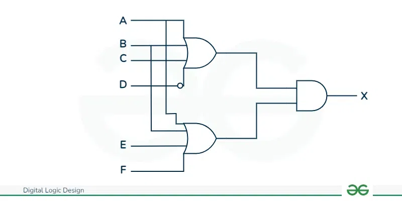
6. Realize W = AB + CD + EF + GH using 2 input NAND gates.
(a) 6
(b) 7
(c) 8
(d) 9

NAND gate realization
Explanation:
Let’s realize W logical expression by using 2 input NAND gates.
We can see (AB)‘ is an output expression of NAND gate 1.
Similarly, (CD)‘ and (EF)‘ are the output expression of NAND gates 2 and 3.
Now, we use NAND gate as an Output expression i.e. X = ((AB)‘.(CD)‘)‘ = AB + CD
To find the output expression of NOT gate
i.e. Y, we use Not gate
i.e Y = (AB + CD)‘
Output expression of NAND gate i.e. Z = (EF)‘
Now, To realize the final expression of NAND gate
i.e. W = ((AB + CD)‘ .(EF)’)’
W= AB + CD + EF
We have used minimum 6 NAND gates to realize expression of W.
W = AB + CD + EF is the correct answer i.e. option (a).
7. Simplify f (a , b , c) = [Tex]\sum m[/Tex] (0, 2, 5, 7)
(a) a’c’
(b) a’c’ + a’c
(c) a’c’ + ac’
(d) a’c’ + ac
Explanation:
Let’s make a 3 variable K-map to simplify the Boolean expression:
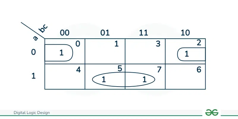
3 variable K-map simplification
We use minterms that represents as 1 to solve the K-Map expressions as:
f = a’ b’ c’ + a’ b c’ + a b’ c + a b c
f = a’ c’ + a c
So, Option (d) is the correct answer.
8. In the given figure, Realize output expression of Y.
(a) 1
(b) 2
(c) 3
(d) 4
Explanation:
Output of XOR gate 1 = X’
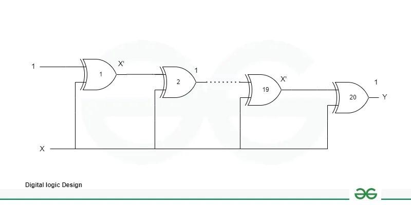
XOR gate simplification
Output of XOR gate 2 = 1
Further, simplification of each output gate results as Y = 1 , So, Option (a) is the correct answer.
9. Find Product of Sum (POS) form of f (a, b, c, d) = πM (1, 4, 6, 9)
(a) (d + a + b’). (b’ + c’ + d’)
(b) (d + a + b’). (b + c + d’)
(c) (d + a + b’). (b’ + c + d)
(d) (d + a + b’). (b + c’ + d’)
Explanation:
Let’s draw a 4 variable K-Map for the given equation:

4 variable K-map simplification
We use maxterms that represents as 0 to solve the K-Map expressions as:
First, make the group of 2 i.e. Group 1 , f1 = (b + c + d’)
Similarly, Group 2 , f2 = (d + a + b’)
f = f1 . f2
where, f is the final expression of K-map to find the POS form.
f = (d + a + b’). (b + c + d’)
i.e. So, Option (b) is the correct answer.
10. Convert (312)8 into decimal
(a) (201)10)
(b) (202)10
(c) (203)10
(d) (204)10
Explanation:
To obtain the Octal to decimal conversion by multiplying 8 to the power of base along with the value at the index position.
(312)8 = 3 * 82 + 1* 81 + 2* 80
= 192 + 8 +2 = (202)10
So, Option (b) is the correct answer.
11. In the toggle mode, a JK flip-flop has
(a) J = 0, K = 1
(b) J = 1, K = 1
(c) J = 0, K = 0
(d) J = 1, K = 0
Explanation:
Let’s see the truth table of JK Flip flop:
Inputs
| Output
|
J
| K
| Q+
|
0
| 0
| Q (Hold)
|
0
| 1
| 0 (Reset)
|
1
| 0
| 1 (Set)
|
1
| 1
| Q'(Toggle)
|
Toggling is the process of applying a clock signal to the output and then switching between the two states. Assume, for instance, that the output state Q of output Q+ will initially be either 1 or 0. Then, after toggling, the output state Q’ of output Q+ will be either X’ or 1.
Both J and K should be 1 for toggle in JK flip flop. So, Option (b) is the correct answer.
12. Calculate the Value of the R from the Expression : (141)R = (997)2
(a) 3
(b) 4
(c) 5
(d) 6
Explanation:
1 x R2 + 4 x R1 + 1 x R0 = 9 x 22 + 9 x 21 + 7 x 20
1 x R2 + 4 x R1+ 1 = 36 + 18 + 7
1 x R2 + 4 x R1 – 60 = 0
On Solving the above equation as:
R2 + 4R- 60 = 0
R2 + 10R – 6R – 60 = 0
R( R+10) -6( R+10 )=0
(R+10)(R-6)=0
R = 6 , -10
So, the value of the R is 6
So, Option (d) is the correct answer.
13. De-Morgan’s Law states that
(a) (A+B)’ = A’*B
(b) (AB)’ = A’ + B’
(c) (AB)’ = A’ + B
(d) (AB)’ = A + B
Explanation:
Digital electronics depends extensively on De-Morgan’s law. It provides an equivalent for each logic gate.
De-Morgan’s theorems come in two different types:
- the first provides the NOR gate equivalent, while
- the second provides the NAND gate equivalent.
According to the De-Morgan’s theorem’s dual property,
(AB)’ = A’ + B’ and (A + B)’ = A’.B’
So, Option (b) is the correct answer.
14. The following hexadecimal number (1E.43)16 is equivalent to
(a) (36.506)8
(b) (36.206)8
(c) (35.506)8
(d) (35.206)8
Explanation:
To Solve this let’s first convert the hexadecimal number into actual number and writes its binary equivalent of each digits in the form of four bits.By doing this we can convert hex decimal number into binary form.Next step is to divide the binary equivalent into three bits and then write the corresponding digit for each of the three bits.
(1E.43)16 = (0001 1110.0100 0011)2
= (00011110.01000011)2
= (011110.010000110)2
= (011 110.010 000 110)2
= (36.206)8
So, Option (b) is the correct answer.
15. Design a counter with sequences 0, 2, 3, 1, 0 using D-flip flops.
(a) D1 = Q0‘ and D0 = Q1‘
(b) D1 = Q0 and D0 = Q1
(c) D1 = Q0 and D0 = Q1‘
(d) D1 =Q0‘ and D0 = Q1
Explanation:
Let’s design a counter sequences 0, 2, 3, 1, 0 using D-flip flops:
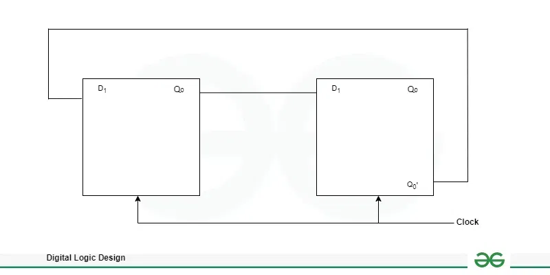
Counter using D Flip-flops
Let’s draw a truth table to find the next states with given sequences:
Present State
| Next State
| Output
|
Q1Q0
| Q1+Q0+
| D1D0
|
00
| 10
|
10
|
10
| 11
| 11
|
11
| 01
| 01
|
01
| 00
| 00
|
Let’s draw Sequence counter and it’s equivalent K-map:
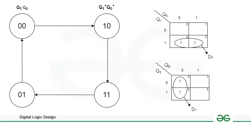
Sequence counter using D Flip-flops and K-map simplification
Let’s make a given sequence with considering Q1Q0 are the initial states of a sequence counter and Q1 + Q0 + are next states of a sequence counter.
D1 and D2 are the final outputs of D-Flip flops.
After obtaining the truth table of given sequence, we have observed a 1 variable K-map for D1 and D2
So, D1 = Q0‘ and D2 = Q1
i.e., So, Option (d) is the correct answer.
16. Consider the 2-bit multiplexer (MUX) shown in the figure. For OUTPUT to be the XOR of C and D, the values for A0, A1, A2 and A3 are ?
(a) A0 = 0, A1 = 1, A2 = 1, A3 = 0
(b) A0 = 0, A1 = 0, A2 = 1, A3 = 0
(c) A0 = 0, A1 = 1, A2 = 0, A3 = 0
(d) A0 = 1, A1 = 1, A2 = 1, A3 = 0
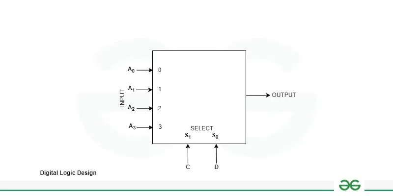
2-bit Multiplexer
Explanation:
The output of Multiplexer, F is
F = S1’S0’ I0 + S1’S0 I1 + S1S0’ I2 +S1S0 I3
F = C’D’A0 + C’DA1 + CD’A2 + CDA3
But output, F = C XOR D = C’D + CD’ ( A0 A1 A2 A3 )
Inputs of Multiplexer are, A0 = 0, A1 = 1, A2 = 1, A3 = 0 ,
i.e. , Option (a) is the correct answer.
17. Which of the following option input sequences for a cross-coupled R-S latch realized with two NOR gates may lead to an oscillation?
(a) 11, 00
(b) 01, 10
(c) 10, 015
(d) 00, 11
Explanation:
Let’s draw a cross-coupled R-S latch realized with two NOR gates along with R-S latch truth table:
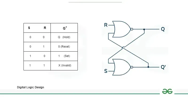
S-R latch using 2 NOR Gates and SR latch truth table
Let’s understand the property of NOR Gates:

Property of NOR Gates
As we know the truth table of SR latch, with different input conditions of SR, it may lead to 2 output states
i.e. Q = Hold on the same state and
Q+ = invalid state that both input conditions results in oscillation.
By using the property of NOR gate: we can understand how to apply input on cross-coupled NOR gates.
NOR gates are used in the RS latch. The indeterminate state came through a 00 input case may result in an oscillation. i.e. option (d) is the correct answer.
18. If both S and R inputs of an SR latch formed by cross-coupling two NOR gates are set to 0, the output is
(a) Q = 0, Q’ = 1
(b) Q = 1, Q’ = 0
(c) Q = 1, Q’ = 1
(d) Indeterminate states
Explanation:
Let’s draw a cross-coupled R-S latch realized with two NOR gates along with R-S latch truth table:

S-R latch using 2 NOR Gates and SR latch truth table
Let’s understand the property of NOR Gates:

Property of NOR Gates
With different input conditions of SR, it may lead to 2 output states
i.e. Q = Hold on the same state and
Q+ = invalid state that both input conditions results in oscillation.
By using the property of NOR gate: we can understand how to apply input on cross-coupled NOR gates.
When R and S are both set to 0, we obtain Q and Q’ as 1.
This output will be permanent and only be affected by the input values [No Race Around Condition].
It will not be impacted by the order in which the events occurs.
The output would be uncertain if we changed R = S = 1 after this stage, though, as it would depend on which NOR gate processes first (either Q or Q’ will become 0, but we can’t assure which Race Around Condition is indeterminate state).
i.e. option (c) is the correct answer.
19. A traffic signal cycles from GREEN to YELLOW, YELLOW to RED and RED to GREEN. In each cycle, GREEN is turned on for 70 seconds, YELLOW is turned on for 5 seconds and the RED is turned on for 75 seconds. This traffic light has to be implemented using a finite state machine (FSM). The only input to this FSM is a clock of 5 second period. The minimum number of flip-flops required to implement this FSM is ?
(a) 5
(b) 4
(c) 6
(d) 7
Explanation:
Green is turned ON for 70 seconds
Yellow is turned ON for 5 seconds.
Red is turned ON for 75 seconds
∴ Total time to complete one cycle for all 3 lights = (70 + 5 +75) seconds = 150 seconds
Available time period of clock = 5 seconds
Total number of clock cycles in one complete cycle = 150/5 = 30
Assume number of flip-flops required = n
Using n flip-flops = 2n,
we may calculate the maximum number of states. Thus, to obtain 30 states or 30 clock cycles,
2n ≥ 30
⇒ n ≥ 4.90
∴ Minimum number of required flip-flops is = 5
i.e. option (a) is the correct answer.
20. Assuming that all flip-flops are in reset condition initially, the count sequence observed at QA in the circuit shown is
(a) 0010111…
(b) 0001011…
(c) 0101111…
(d) 0110100…
Explanation:
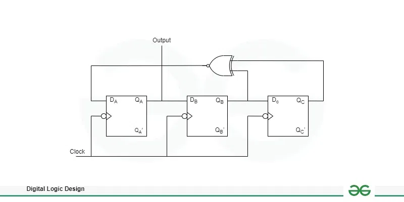
Three D Flip-flops with a XNOR gate
In the given circuit, a circuit consists of three D Flip-flops with a XNOR gate and a clock signal is applied as synchronous.
We have to obtain count sequence at Output QA. Assuming initially all flip-flops are in reset condition. DA DB Dc QA’ QB’ QC’
Initially, QC, QB, and QA are “0.” As a result, DA = ‘1’. QA becomes “1” with the first clock pulse. QB and QC stay in the state of logic “0.” DA remains at 1.
After the second clock pulse, QA is still in the logic-‘1’ condition. QB turns becomes a “1.” QC stays at zero. DA drops to ‘0’.
The third clock pulse causes QA to change to “0.” Therefore, 0110 is the first four entries of QA.
0110100…is the count sequence observed at QA i.e. option (d) is the correct answer.
21. The full-scale output of a digital to analog converter is 20 mA. If the resolution is 80µA, then the minimum number of bits required and percentage resolution are:
(a) 0.8
(b) 0.07
(c) 3.9
(d) 0.39
Explanation:
The following provides the resolution for n bit Digital to analog converter (DAC):
R = Vref / 2n-1
The following provides the % resolution for n bit DAC:
% R = (1 / 2n-1 ) * 100
80 * 10-6 = ( 20 * 10-3 ) / ( 2n-1 )
n = 8 and % R = (1 / 28-1 ) * 100 , where, the minimum number of bits required, n = 8
So, the percentage resolution, % R = 0.39
So, option (d) is the correct answer.
22. If the resolution of a digital-to-analog converter is approximately 0.4% of its full-scale range, then it is:
(a) 16-bit converter
(b) 10-bit converter
(c) 8-bit converter
(d) 12-bit converter
Explanation:
Resolution can be defined as the Smallest amount of changes in the analog output voltage which results change of one bit in the output.
To solve the above question ,now Let’s first examine the relationship between resolution and the bit count of a Digital-to-analog converter (DAC) in order to choose the Correct response.
The smallest change in the output voltage that a DAC is capable of producing is referred as a resolution. Usually, a percentage of the full-scale range is used to express it.
Let’s denote:
R : Resolution (0.4% of full-scale range in this case) , N as the number of bits in the DAC
The relationship between resolution and the number of bits is given by the formula:
R = 100% / 2N
Given, Resolution R is 0.4% (0.004 in decimal form), we need to find the value of N.
0.004 = 100% / 2N
To solve for N, we can take the logarithm base 2 on both sides:
log2 (0.004) = log2 (100% / 2N)
log2 (0.004) = log2 (100%) – log2 (2N)
log2 (0.004) = 0 – N log2 (2)
log2 (0.004) = – N
N = – ( log2 (0.004) / log2 (2) )
N ~ – 8.6439 / 1 ~ 8.6439
Since the number of bits must be a whole number, the most appropriate answer is 8 bits.
So, option (c) is the correct answer.
23. A MOD-16 ripple counter using J-K flip-flop has a current state 1001. What will the state be after 31 clock pulses?
(a) 1001
(b) 1010
(c) 1000
(d) 1111
Explanation:
Given, The current state of a MOD-16 ripple counter that uses a J-K flip-flop is 1001 so, the possible values of a MOD-16 ripple counter is 0 to 15. Thus, after 31 clock pulses, the present binary value 1001, or the corresponding decimal value 11, becomes (11 + 31) = 42 logically.
Now, after 31 clock pulses, the final state is a remainder of decimal 10 or binary 1000, which we can obtain by dividing 42 by 16. So, option (c) is the correct answer.
24. A specific counter is using five S-R flip-flops. So what is the maximum number of states possible?
(a) 4
(b) 16
(c) 32
(d) 64
Explanation:
A particular counter is utilizing five S-R flip-flops so, the maximum number of states that may be achieved by a counter is given by 2n with n number of flip-flops.
Thus, 25 = 32 is the maximum number of states. So, option (c) is the correct answer.
25. What is the maximum delay that can occur if four flip-flops are connected as a ripple counter and each flip-flop has propagation delays of tPHL = 22 ns and tPLH = 15 ns?
(a) 15 ns
(b) 22 ns
(c) 60 ns
(d) 88 ns
Explanation:
The maximum delay between an input changing value and an output changing value is the largest delay which is known as the maximum propagation delay.
tpHL : It is a propagation delay when output switches from (High to Low)
tpLH : It is a propagation delay when output switches from (Low to High)
The largest delay possible when connecting four flip-flops to form a ripple counter as there are four FFs, 22 * n = 22 * 4 = 88 ns. So, option (d) is the correct answer.
26. The logic gates shown in the given figure works as:
(a) decoder
(b) binary to EXCESS-3 converter D3 D2 D1 D0
(c) priority encoder
(d) binary to gray converter

Priority encoder
Explanation:
Priority encoders are used to overcome the issue where an encoder produces an output that may not be accurate if several inputs are high.
To determine whether or not the code available at outputs is valid, we took into consideration one additional output, V. A valid code can be found at the outputs of the encoder if at least one of its inputs is ‘1’.
In this instance, V, the output, will equal to 1 If the encoder inputs are all “0,” the code that appears at the outputs is invalid. In this instance, V, the output, will equal 0.
Inputs
|
Outputs
|
|---|
Y3
|
Y2
|
Y1
|
Y0
|
A1
|
A0
|
V
|
|---|
|
0
|
0
|
0
|
0
|
0
|
0
|
0
|
|---|
|
0
|
0
|
0
|
1
|
0
|
0
|
1
|
|---|
|
0
|
0
|
1
| x
|
0
|
1
|
1
|
|---|
|
0
|
1
| x
| x
|
1
|
0
|
1
|
|---|
|
1
| x
| x
| x
|
1
|
1
|
1
|
|---|
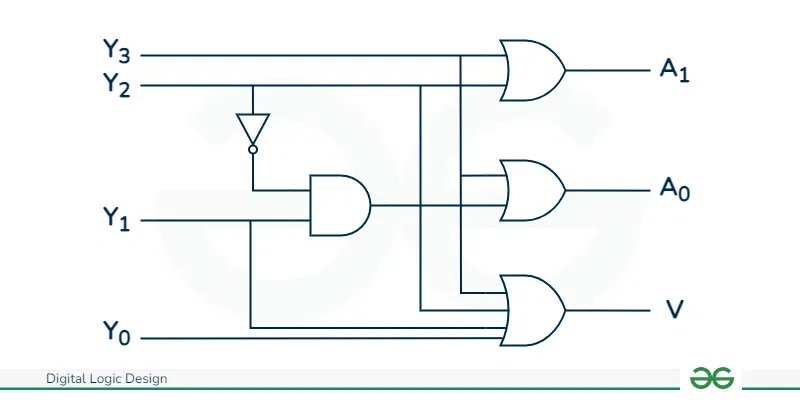
Priority encoder
Explanation:
Logic shown in given figure will work as Priority encoder (4 × 2) Inputs = D3, D2, D1 , D0
Output: Y = D3 + D2 ’ D1 X = D3 + D1 V = D3 + D2 + D1 + D0
Thus, option C is the correct answer.
27. Which of the circuits in figure (a to d) is the sum-of-products?
(a) a
(b) b
(c) c
(d) d

Option (a)
Option (b)

Option (c)
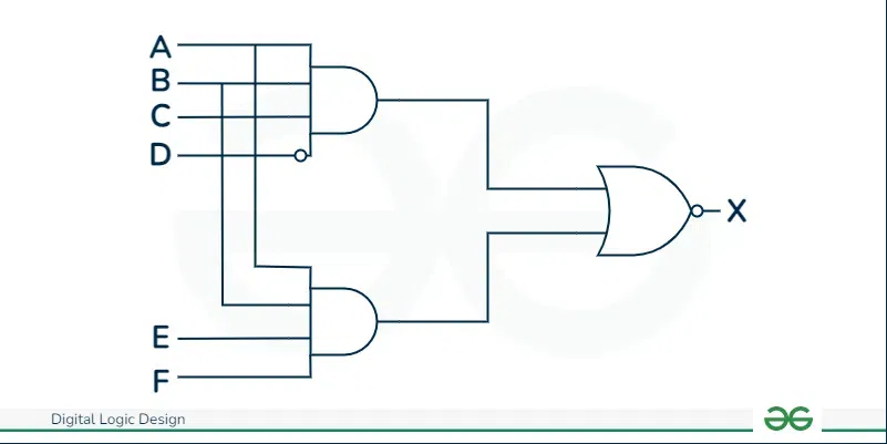
Option (d)
Explanation:
Sum of Products, or SOP form, is a representation of the sum of product terms with variables in both complemented and uncomplemented form. The diagram of figure d is in SOP form because it has the AND gates after the OR gates.
An expression that combines several product terms—each of which may contain variables in both complemented and uncomplemented forms—is known as the sum of products (SOP). Because Figure D’s schematic reflects this expression structure by placing the AND gates after the OR gates, it is in SOP form. Thus, option D is the correct answer.
28. The device shown here is most likely ?
(a) Comparator
(b) Multiplexer
(c) Inverter
(d) Demultiplexer

Demultiplexer
Explanation:
The provided diagram is a demultiplexer since it accepts a single input and produces numerous outputs. A combinational circuit known as a demultiplexer latches one output to multiple outputs based on select lines.
A demultiplexer comprises one input line, n control input lines (also known as address or select lines), and 2n output lines. The number of possible output channels and the number of output lines match.
Thus, option D is the correct answer.
29. In a combinational circuit, the output at any time depends only on the _______ at that time.
(a) Voltage
(b) Intermediate values
(c) Input values
(d) Clock pulses
Explanation:
A combinational circuit’s output depends entirely on its input values at any given moment so it is not dependent on values from the past or present.
The output of a combinational circuit depends entirely on the input values present at that particular moment.
Thus, option C is the correct answer.
30. If the two numbers include a sign bit in the highest order position, the bit conditions of interest are the sign of the result, a zero indication and ___________
(a) An underflow condition
(b) A neutral condition
(c) An overflow condition
(d) One indication
Explanation:
The bit criteria are the result’s sign, a zero indicator, and an overflow condition if the two numbers have a sign bit in the highest order position.
The conditions that are relevant would be the sign of the result, a zero indication, and an overflow condition if we were analyzing two numbers with a sign bit in the highest order position.
Thus, option C is the correct answer.
31. A sequence of equally spaced timing pulses may be easily generated by which type of counter circuit?
(a) Ring counter
(b) Clock
(c) Johnson
(d) Binary
Explanation:
The input of the flip-flop is fed to the feedback from its output in a ring counter. As such, it produces timing pulses that are uniformly spaced.
Every flip-flop in a ring counter is connected to the input of the next flip-flop.
A series of timing pulses is produced when clock pulses are delivered because the logic level—high or logic level- low which circulates through the flip-flops in a cyclic manner.
Because the flip-flops are connected to form a closed loop, or ring, the timing pulses are uniformly spaced.
Thus, option A is the correct answer.
32. A bidirectional 4-bit shift register is storing the nibble 1101. Its input is HIGH. The nibble 1011 is waiting to be entered on the serial data-input line. After three clock pulses, the shift register is storing ________
(a) 1101
(b) 0111
(c) 0001
(d) 1110
Explanation:
It is a right shift register when the mode is high. The bit that remain in the register is 1 and after three clock pulses enter bits are 011. 0111 is hence the necessary solution.
Given the initial state of the register is 1101 and the input is HIGH, let’s see the changes after three clock pulses:
1011→ Right shift→ 1101 (After Clock Pulse 1, It is a right shift register when the mode is high)
Clock Pulse 2: 1101 → Right shift → 1110 (LSB is shifted out, and the input bit is shifted in).
Clock Pulse 3: 1110 → Right shift → 0111.
Thus, option B is the correct answer.
33. How many different states does a 3-bit asynchronous down counter have?
(a) 2
(b) 4
(c) 6
(d) 8
Explanation:
Let’s first define an asynchronous down counter in order to determine how many possible states a 3-bit asynchronous down counter can have.
One type of digital counter circuit that counts down from initial value to zero is an asynchronous down counter. A 3-bit asynchronous down counter decrements by 1 with each clock pulse as it cycles through a series of states, with each flip-flop representing one bit.
The total number of possible combinations of a 3-bit asynchronous down counter’s three bits determines the number of various states that the counter can have. Since each bit has a possible value of 0 or 1.
In a n-bit counter, the total number of states = 2n.
Therefore, in a 3-bit counter, the total number of states = 23 = 8 states.
Thus, option D is the correct answer.
34. In a 3-bit asynchronous down counter, at the first negative transition of the clock, the counter content becomes ____________
(a) 000
(b) 111
(c) 101
(d) 010
Explanation:
The counter content of a 3-bit asynchronous down counter decreases by one at the first negative clock transition.
Because each negative transition in the down counter causes the counter content to decrease by one. Therefore, in a 3-bit asynchronous down counter, the counter content changes to 111 at the clock’s first negative transition. Thus, option B is the correct answer.
35. In JK flip flop same input, i.e. at a particular time or during a clock pulse, the output will oscillate back and forth between 0 and 1. At the end of the clock pulse the value of output Q is uncertain. The situation is referred to as?
(a) Conversion condition
(b) Race around condition
(c) Lock out state
(d) Forbidden State
Explanation:
In the JK Flip Flop if the same input is given at a Specific time or during a clock,the output of the jk flip flop will fluctuate between 0 and 1 Which leads to undefining of the Value at the output Q by the end of the pulse and this situation is know as race around condition.
So in the question,the system or device will try to carry out two or more operation simultaneously,due to the nature of the system or device the task must be completed in the correct order which will lead to an undesirable situation known as race condition,So in the given option B is the correct answer.
36. Which of the following flip-flops is free from race around condition?
(a) All of the above
(b) T flip-flop
(c) SR flip-flop
(d) Master slave JK flip-flop
Master Slave JK flip-flop
Explanation:
Every time an applied input changes at a high clock, the output also changes. However, in a JK flipflop, the race-around condition occurs when J = K = 1 and the output changes without any change in the input.
When the clock signal is “HIGH,” the circuit accepts input data and sends it to the output on the clock signal’s falling edge. Stated differently, the Master-Slave JK Flip flop is a “Synchronous” device since it exclusively transfers data in accordance with the clock signal’s timing.
The JK flip flop is the most adaptable flip flop and is most frequently utilized when implementing an arbitary state machine with discrete components.
Master slave JK flip-flops is free from race around condition.
Thus, option D is the correct answer.
37. What type of logic circuit is represented by the figure shown below?
(a) XOR
(b) XNOR
(c) AND
(d) XAND

XNOR gate realization
Explanation:
Let’s analyse the given circuit and solve the expressions obtain as per each operations is applied on the gate.
A’ and B’ are the inputs fed to the AND gate and A’.B’ is the first input of OR gate and A.B is the another input fed to the OR gate.
Then, After solving the circuit , X is the output of OR gate, X = A’.B’ + A.B that represents boolean expression of XNOR gate.
Thus, it will produce 1 when inputs are even number of 1s or all 0s, and produce 0 when input is odd number of 1s.
Thus, option B is the correct answer.
38. For realisation of JK flip-flop from SR flip-flop, the input J and K will be given as ___________
(a) External inputs to S and R
(b) Internal inputs to S and R
(c) External inputs to combinational circuit
(d) Internal inputs to combinational circuit
Explanation:
If a JK Flip Flop is required, the inputs feed into the combinational circuit, and the flip flop’s inputs are connected to the combinational circuit’s output.
J and K are then provided to S and R as external inputs. While JK flip-flops do not have an invalid state, SR flip-flops do.
So, For realisation of JK flip-flop from SR flip-flop, the input J and K will be given as External inputs to S and R.
Thus, option A is the correct answer.
39. The only difference between a combinational circuit and a flip-flop is that _____________
(a) The flip-flop requires previous state
(b) The flip-flop requires next state
(c) The flip-flop requires a clock pulse
(d) The flip-flop depends on the past as well as present states
Explanation:
Because the outputs of combinational circuits are updated instantaneously based on the input values, they do not require a clock signal.
Latches and flip-flops are two types of memory elements that have clock and control inputs. Both the past and the present states are essential for them. In contrast, combinational circuits only depend on the current state.
Due to this ,the major difference between a flip-flop and a combination circuit is that the flip flop requires a clock pulse to operate as an timing mechanism which updates its output at specific intervals and accepts new input values. Thus, option C is the correct answer.
40. For a 4 bit MOD-16 ripple counter using J-K flip-flop, the propagation delay of each flip flop is 50ns. What is the maximum clock frequency can be used?
(a) 10 MHz
(b) 20 MHz
(c) 5 MHz
(d) 40 MHz
Explanation:
Given, For a 4 bit MOD-16 ripple counter using J-K flip-flop, the propagation delay of each flip flop is 50ns.
Total propagation delay for 4 flip-flops (1 bit for each) = (4 × 50 ns) = 200ns
So, maximum clock frequency is reciprocal to the total propagation delay = (1 / (200 × 10-9)) Hz = 0.005 * 109 Hz
Maximum clock frequency = 5 × 10⁶ Hz= 5 MHz
Thus, option C is the correct answer.
41. How many 3 to 8 line decoders are required for a 1 of 32 decoder?
(a)1
(b)2
(c)4
(d)8
Explanation:
The output of a 3 to 8 line decoder gives 8 output lines.
In order to produce 32 output lines, 32/8 = 4 (3 to 8 line decoders) are required.
Based on a 2-bit input code that is obtained from the remaining address lines, each decoder will turn on.
The final 32 output lines can be obtained by combining the output lines of all four decoders using OR gates.
Total 4 (3 to 8 line decoders) are required So, option (c) is the correct answer.
42. Which of the following is correct for a gated D-type flip-flop?
(a) The output toggles if one of the inputs is held HIGH
(b)Only one of the inputs can be HIGH at a time
(c)The output complement follows the input when enabled
(d)Q output follows the input D when the enable is HIGH
Explanation:
An enable input (also referred to as “EN”) is requried as an input in a gated D flip-flop. It is employed to regulate the flip-flop’s behavior and choose which saves time and determine the input data. The clock input (also referred to as “CLK”) and the data input (also referred to as “D”) are the two primary inputs of the D flip-flop. “Q” represents the flip-flop’s output.
When the enable input (EN) is HIGH, the gated D flip-flop stores the input data (D) on the rising edge of the clock signal (CLK). – The flip-flop ignores any changes in the input data (D) and maintains the same output (Q) when the enable input (EN) is LOW.
When the clock signal rises and the enable input (EN) is HIGH, the output (Q) follows the input (D).The correct option is option ‘D’
43. Whose operations are more faster among the following?
(a) Combinational circuits
(b) Sequential circuits
(c) Latches
(d) Flip-flops
Explanation:
Sequential circuits are slower than combinational circuits as Combinational circuits function without the requirement for memory elements, whereas sequential circuits which include latches and flip-flops need memory devices in order to carry out their operations sequentially.
As their is no feedback in the sequential circuit which introduces delays in sequential circuits,So the Combinational circuits are Faster. Combinational circuit also has benifts like parallelism, have simpler structures, and also has shorter propagation delays. However, the relative speed can only depends on the specific design and optimization of each circuit type.
So, option (a) is the correct answer.
44. As the number of flip flops are increased, the total propagation delay of __________
(a) Ripple counter increases but that of synchronous counter remains the same
(b) Both ripple and synchronous counters increase
(c) Both ripple and synchronous counters remain the same
(d) Ripple counter remains the same but that of synchronous counter increases
Explanation:
In the Ripple counter the each flip flop is triggered bt the output of the previous flip as each flip-flop adds a delay of its own, which adds up as the signal propagates through the counter,So the total propagation delay increases as the number of flip-flops increases.
On the other hand, a clock signal triggers each flip-flop in a synchronous counter simultaneously. Consequently, there is no addition of delays as observed in ripple counters, and the overall propagation delay is constant regardless of the number of flip-flops as each flip-flop experiences the same delay.
Therefore, a synchronous counter’s overall propagation latency remains constant while total propagation delay of a ripple counter’s increases with the number of flip-flops.Clock pulses are applied to a single flip-flop in a ripple counter. Therefore, the latency increases with the number of flip-flops. Clock pulses are applied concurrently to each flip-flop in the synchronous counter.
So, option (a) is the correct answer.
45. An asynchronous binary up counter, made from a series of leading edge-triggered flip-flops, can be changed to a down counter by ________
(a) Taking the output on the other side of the flip-flops (instead of Q)
(b) Clocking of each succeeding flip-flop from the other side (instead of Q)
(c) Changing the flip-flops to trailing edge triggering
(d) All of the Mentioned
Explanation:
We can apply any or all of the following changes to change an asynchronous binary up counter, which is composed of leading edge-triggered flip-flops into a down counter:
a) Consider the output on the other side of the flip-flops (rather than Q): This makes the counting sequence into a down counter by effectively reversing it.
b) Clock each subsequent flip-flop from the opposite side (instead of Q): You can flip the counter’s counting direction by altering the clocking technique.
c) Convert the flip-flops to trailing edge triggering: This would essentially reverse the counting orientation from up to down. Trailing edge triggered flip-flops trigger on the clock signal’s falling edge.
The Asynchronous Binary up counter are made from the leading edge-triggered flip – flops that can be changed to a down counter.This Flip Flops are also referred as Flip Flops that are triggered during a clock transition from LOW to HIGH or HIGH to LOW.
So, option (d) is the correct answer.
46. A 4-bit binary up counter has an input clock frequency of 20 kHz. The frequency of the most significant bit is ________
(a) 1.25 kHz
(b) 2.50 kHz
(c) 160 kHz
(d) 320 kHz
Explanation:
Given, A 4-bit binary up counter has an input clock frequency of 20 kHz. For a 4-bit counter, the count frequency is 10 kHz when the input clock frequency of 20 kHz / 2 is divided.
The most significant bit (MSB) changes state at the 8th stage because each bit represents a binary value of powers of 2 (1, 2, 4, 8 for the first, second, third, and fourth bits, respectively).
We further divide this count frequency by 8 to determine the frequency of the most significant bit, since the MSB changes state at the eighth stage.
Hence, Frequency of MSB = 10 KHz / 8 = 1.25 kHz. So, option (a) is the correct answer.
47. How many address bits are required to select memory location in the Memory decoder?
(a) 4 KB
(b) 8 KB
(c) 12 KB
(d) 16 KB
Explanation:
Based on the memory’s capacity, you must calculate the number of address bits needed in order to choose memory locations in a memory decoder.
Given that the RAM and EPROM both have a 4 KB capacity, which is equivalent to 4 * 1024 = 4096 memory locations.
Because 212= 4096, you require 12 address bits to address 4096 memory locations.
Memory decoder decodes the memory to be selected for a specific address. Since the given EPROM and RAM are of 4 KB (4 * 1024 = 4096) capacity, it requires 12 address bit to select one of the 4096 memory locations. So, option (c) is the correct answer.
48. How many 16K * 4 RAMs are required to achieve a memory with a capacity of 64K and a word length of 8 bits?
(a) 2
(b) 4
(c) 6
(d) 8
Explanation:
In order to obtain 64K of memory with an 8-bits word length, you can compute the entire amount of memory needed in bits and then figure out how many 16K * 4 RAMs are required.
Given, capacity required is 64K.
Word length is 8 bits.
Total memory required = Capacity * Word length = 64K * 8 bits = 512K bits
Let’s now calculate the number of 16K * 4 RAMs required:
The capacity of each 16K * 4 RAM is 16K * 4 = 64K bits.
So, the number of 16K * 4 RAMs required = Total memory required / Capacity of each RAM = 512K / 64K = 8.
To produce a memory with a capacity of 64K and a word length of 8 bits, you would therefore require 8 (16K * 4 RAMs). . So, option (d) is the correct answer.
49. The complex programmable logic device contains several PLD blocks and __________
(a) A language compiler
(b) AND/OR arrays
(c) Global interconnection matrix
(d) Field-programmable switches
Explanation:
A global connectivity matrix and many Programmable Logic Device (PLD) blocks are the usual components of Complex Programmable Logic Devices (CPLDs).
The Fundamental CPLD Programmable logic components are known as PLD Block.They contains components like flip-flops, arrays of programmable logic gates, and other configurable components.
The Matrix which helps to route and communicate between Various PLD blocks and other CPLD components are known as Global Interconnection Matrix.Complex routing configurations are possible because to the flexible coupling between different logic components that it allows.
Global Interconnection allows the general functionality and versatility of CPLDs, even though they may contain other components like memory blocks, I/O blocks, and dedicated hardware for particular tasks.
So, option (c) is the correct answer.
50. The difference between a PAL & a PLA is ____________
(a) PALs and PLAs are the same thing
(b) The PLA has a programmable OR plane and a programmable AND plane, while the PAL only has a programmable AND plane
(c) The PAL has a programmable OR plane and a programmable AND plane, while the PLA only has a programmable AND plane
(d) The PAL has more possible product terms than the PLA
Explanation:
Programmable Array Logic, or PAL:
A PAL usually consists of a programmable AND plane and a fixed OR plane. The programmable AND plane Which allows the customisation of logic functions by configuration between input and the AND gate connections.
The connections between the AND gates’ output and the OR gates, are predefined and cannot be changed because the OR plane is fixed.
Programmable Logic Array, or PLA:
A PLA contains a programmable AND plane and a programmable OR plane.
Because the AND and OR planes can both be programmable So, constructing complex logic operations is much more flexible.
Compared to PALs, a wider range of logic functions can be realized as a result.
The main difference between PAL & PLA is that PLA has a programmable OR plane and a programmable AND plane, while the PAL only has a programmable AND plane and a fixed OR plane.
So, option (b) is the correct answer.
Share your thoughts in the comments
Please Login to comment...