Clock Skew in synchronous digital circuit systems
Last Updated :
22 Dec, 2022
In Synchronous circuits where all the logic elements share the same clock signal, it becomes imperative to design these elements as close to the clock source as possible because a system-on-chip, FPGA, CPLD contain Billions of transistors. Even though these distances are minute due to their sheer number there is a propagation delay which leads to the clock signal arriving at different parts of the chip at different times. This is called Clock Skew.
In Digital Circuit Design a ” Sequentially Adjacent ” circuit is one where if a pulse emitted from a common source is supposed to arrive at the same time. Using this definition we can write a mathematical expression for clock skew as
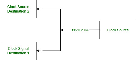
Sequentially Adjacent Circuit

Non-Sequentially Adjacent Circuit.
Ta(Time of arrival of clock pulse at component a)
Tb(Time of arrival of clock pulse at component b)
Then,
Clock skew Ts = Ta - Tb
Factors causing Clock Skew :
- Interconnect Length
- Temperature Variations
- Capacitive Coupling
- Material Imperfections
- Differences in input capacitance on the clock inputs
Types of Clock Skew :
- Positive Skew –
This occurs when the receiving register receives the clock pulse later than it is required.
- Negative Skew –
This occurs when the receiving register receives the clock pulse earlier than required.
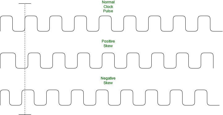
Types of Clock Skews
Share your thoughts in the comments
Please Login to comment...