VLSI Design Cycle
Last Updated :
02 Dec, 2022
Very Large Scale Integration(VLSI) is the process of making Integrated Circuits (ICs) by combining a number of components like resistors, transistors, and capacitors on a single chip.
VLSI Design is an iterative cycle. Designing a VLSI Chip includes a few problems such as functional design, logic design, circuit design, and physical design. The design is verified for accuracy by the process of simulation. If any design errors are found at any stage of verification, at least one of the previous design steps must be repeated to correct the error during the process of designing.
Description of VLSI Design Flow Chart:
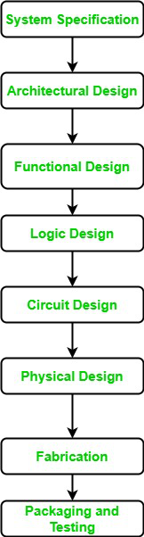
VLSI Design Cycle
1. System specification: The objective of the desired final product is written in this step. During system specification, the designated cost of the system, its performance, architecture, and how the system will communicate with the external world are to be determined. During this step, the design specification should be provided by the users or clients.
2. Architectural design: The basic architecture of the desired design must meet the system specifications of the desired design. The architecture of the desired design is decided and the layout for the same is designed by design engineers. Architectural design includes the integration of analog and mixed-signal blocks, memory management, internal and external communication, power requirements, and choice of process technology and layer stacks.
3. Functional design or Behavioural design: It consists of refining the design specification of the desired design in order to design the functional behavior of the desired system. The main objective of this is to generate design a high-performance architectural design within the cost requirements posed by the specifications.
4. Logic Design: In this step, the structure of the desired design is added to the behavioral representation of the desired design. The main specifications to be considered for logic design are logic minimization, performance enhancement, and testability. Logic design must also consider the problems associated with test vector generation, error detection, and error correction. Many logic synthesis tools have been developed for the automation of the process of logic design.
5. Circuit Design: In this step, the logic blocks of the desired design are replaced by the electronic circuits, which are consists of electronic devices such as resistors, capacitors, and transistors. Circuit simulation of the desired design is done at this stage, in order to verify the timing behavior of the desired system. Kirchhoff’s laws are used to know the behavior of the electronic circuit in terms of node voltages and branch circuits. The result of integrodifferential equations is then solved in discrete- time. SPICE is a well-known program for circuit simulation.
6. Physical Design: In this step, the actual layout of the desired system is done, where all the components will be placed in the circuit and all these components are interconnected. The actual layout of the desired system can affect the area, correctness, and performance of the final desired product. The correctness of the chip is also controlled by the physical design. A circuit design that passes the test of a circuit simulator may be faulty after it has been packaged. This is because of geometric design rule errors. These design rules must be followed to ensure the correctness of the chip fabrication. Errors such as short circuits, open circuits, open channels, etc may result if the design rules are not respected.
7. Fabrication: After the actual layout and verification of the desired design, the design is sent for manufacturing. The handoff of the desired design to the manufacturing process is called tapeout. Generation of the data for manufacturing is referred to as streaming out. The desired design is onto the different layers of the design using the photolithographic process. ICs are manufactured on round silicon wafers with a diameter from 200mm to 300mm, these ICs are then tested and are marked as either functional or defective ICs.
8. Packaging and Testing: After fabrication of desired design, functional chips are then packed. Packaging is configured early in the desired design process and the application along with the cost and form factor requirements. Packaged types may include Dual In-Line Packaged (DIPs), Pin Grid Array (PGAs), and Ball Grid Arrays (BGAs). After a die is positioned in the package cavity, its pins are connected to the pins of the package, e.g., with wire bonding or solider bumps (flip-chip). The package of the desired design is then sealed and then sent to the end-users or clients.
Share your thoughts in the comments
Please Login to comment...