The use of transistors is increasing in modern times, as they are used in amplifier, switches, signal processors, etc. In electronics, the junction field effect transistor is a fundamental component, operating on the principle of electric field control. It is a three-terminal device, and it consists of the gate, drain, and source terminals. The gate serves as the triggering terminal, regulating the flow of current between the drain and source terminals. It is used in amplifier circuits. There are two types of JFETs: N-channel JFET and P-channel JFET. The N channel JFET controls the flow of current through electrons, while the P channel JFET depends on the movement of the holes where the electrons are absent. The gate terminal plays a major role in conducting current and controls the electron flow from source to drain. JFETs are also useful in switching circuits because they can be used as voltage-controlled resistors. This article will discuss the usage functions, features, and characteristics of junction field effect transistors in brief.
What is JFET?
It is the electrical circuit or we can say a voltage driven circuit that means JFET is a three terminal unidirectional electrical circuit. These electronic devices come in various types, including junction field effect transistors (JFETs), N-channel, and P-channel variants. They control the current by manipulating the charge carrier’s movement, which is essential for amplification, switching and an analogue circuit.
JFET
One type of field effect transistor is the junction field impact transistor. In 1953, the first junction field effect transistor was made. In applications where the input impedance needs to be very strong, a junction field effect transistor is used. The junction field effect transistor is known as a unidirectional device because the current flow is only on majority carriers, while in other types, Both majority and minority carriers can benefit from the current flow. Due to their low power consumption, they are more efficient and consume a small amount of power. Due to its low power dissipation, the junction field effect transistor is capable of replacing BJTs and increasing their total efficiency. Because of their high input impedance, they can also replace the BJTs.
Key Terminologies
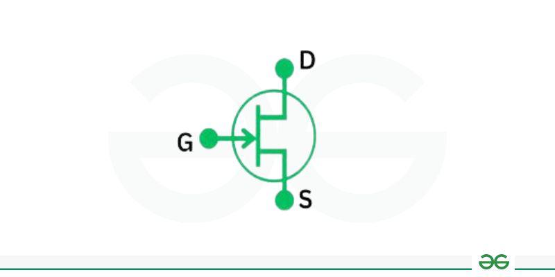
- Junction field effect transistor (JFET): Junction field effect transistor is a three terminal semiconductor device consisting of a gate, a drain, and a source. These can operate on the principle of an electric field, which controls the flow of electrons from source to drain.
- Gate: This terminal plays a significant role in controlling the flow of current through this semiconductor device.
- Source and drain: The source is the terminal where the current enters, and the drain is the terminal where the current exits. The flow of electrons can be controlled by the gate.
- High impedance: The impedance of the JFET is high, which can be suitable for applications like amplifiers where the loading of the input signal of the amplifier is desired.
- Biasing: This is the process of applying an external signal to the gate terminal in JFET to get a specific operating point.
Construction of Junction Field Effect Transistor (JFET)
The junction field effect transistor is a three-terminal semiconductor device that mainly consists of a thin bar of semiconductor material. The material may be silicon or gallium arsenide. The construction of a junction field effect transistor can create a channel in the semiconductor material that acts as a way for the flow of charge carriers. In n-channel JFET, the semiconductor material is n-type, which is doped with impurities. In p-channel JFET, the semiconductor material is p-type with impurities of Holes. The source and drain terminals are known as the two ends of the silicon material, while the third terminal is a gate. The flow of charge carriers is from source to drain, but it does not touch the channel. The gate terminal is separated by a thin insulating layer. The gate triggers this entire circuit, which can control the flow of charge carriers from source to drain.
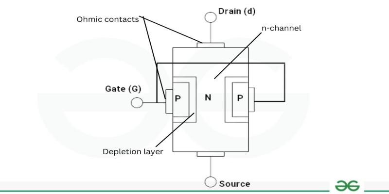
Construction of JFET
Working of Junction Field Effect Transistor
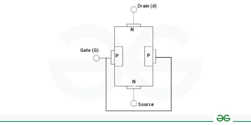
The junction field effect transistor is operated on the current flow through a semiconductor channel. When you apply voltage to a gate, it creates an electrical field but when no voltage is applied then the path becomes the open path for the carriers to flow in that. In the figure, in case of an application of a voltage Vds, two PN junctions are formed on either side by depletion layers to control flow of electrons from source to outflow when gate terminal voltage is zero. The width of these depletion layers can determine the current conduction.
Whenever a reverse voltage Vgs is applied through the gate, the width of the depletion layers increases and raises the resistance of the conduction channel. If voltage Vgs are reduced, the width of layers will decrease. The flow of electrons from the source to the drain will decrease as the depletion layer increases. The flow of electrons will decrease when the width is decreased. The JFET device is capable of controlling the voltage during that process. So in the reverse bias the JFET comes in the cut off region and when the voltage of gate is negative – the width of channel decreases with no current flow through that , which is called pinched off region and the voltage at which this region is obtained is called pinch off voltage.

Working of JFET
Types of JFET
There are two types of JFETs:
- N- channel JFET
- P- channel JFET
N- Channel Junction Field Effect Transistor
The n-channel junction field effect transistor is a semiconductor device that has three terminals: gate, source, and drain. It is made up of an N-type semiconductor thin bar material. The majority of charge carriers for n-type are electrons. This forms a channel between source and drain. When a negative voltage is applied to the gate terminal, it creates an electric field across the insulating material between the gate and the channel. Whenever a negative voltage in the gate increases, the electric field also increases, narrowing the channel and decreasing the current flow between the source and drain. To control the flow of electrons and to be used in applications such as voltage regulator, impedance switches, etc., the high input of this n channel JFET can be used.
n channel JFET
P -Channel Junction Field Effect Transistor
The p-channel junction field effect transistor is a semiconductor device that has three terminals: gate, source, and drain. It is made up of a semiconductor p type thin bar material, The majority of carriers are holes in the p type. This forms a channel between source and drain. When a positive voltage is applied to the gate terminal, it creates an electric field across the insulating material between the gate and the channel. Whenever a positive voltage in the gate increases, the electric field also increases, narrowing the channel and decreasing the current flow between the source and drain. In applications such as amplifiers, switches, and signal processing, the high input of this p channel impedance JFET can be used to control the flow of holes.

p channel JFET
Characteristics of Junction field effect transistor (JFET)
Some of the features that a JFET are listed below:
- Temperature sensitivity: The JFETs are sensitive to temperature variations, which allows them to adapt their properties with changing temperatures. In certain applications, proper thermal management may be necessary.
- Low Noise: JFETs are known for their low noise, which is valuable in applications such as amplifier and sensors where signal integrity is essential.
- High input impedance: The high input impedance of JFETs remains relatively stable over a range of temperatures and voltages, making them suitable for precision applications.
- Variants: JFETs, which allow circuit design flexibility and enable applications that require both sourcing and sinking current, are available in two types of channels: N channel and P Channel.
Other characteristics majorly followed are mentioned below:
- Output characteristics
- Transfer characteristics
Output Characteristics of JFET
The output characteristics of the JFET were plots between drain current (Id) and drain source voltage (Vds). These characteristics find the variation of drain current concerning the voltage applied at the drain-source terminals while keeping the gate-source voltage constant. Basically, the characteristics are of two types: output characteristics, or drain characteristics, and transfer characteristics.
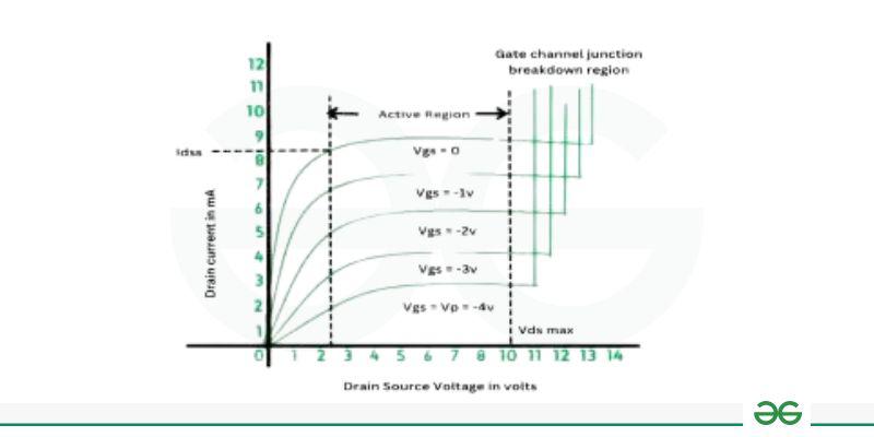
Output characteristics of JFET
Terminologies involved in output characteristics of JFET:
- Saturation region: In this region, the JFET operates with low Vds, and the current is constant. The current is controlled by the gate source voltage (Vgs).
- Ohmic region: JFET becomes an ohmic region with increasing VDS. The drain current increases with Vds.
- Pinched off region: By increasing the VDS, it can lead to a pinch of region; in this region, the channel narrows and the drain current becomes independent of the VDS.
- Breakdown Region: As the voltage of drain source becomes very high then the JFET channels gets breakdown and current flows in a uncontrolled manner.
Transfer Characteristics of JFET
The transfer characteristics of a JFET plotted between the drain current (Id) and drain source voltage (Vds). It can be determined by keeping the Vds constant, and drain current can be observed by changing the gate source voltage. So we can observe that when the gate source voltage Vgs is increased, the drain current Id decreases. When the drain source voltage is constant, it can be observed that the value of the drain current varies inversely with respect to the gate source voltage. The above transfer characteristics curve of JFET is described below; it can be observed that the value of drain current varies inversely with respect to gate-source voltage (vgs) when the drain-source voltage is constant.
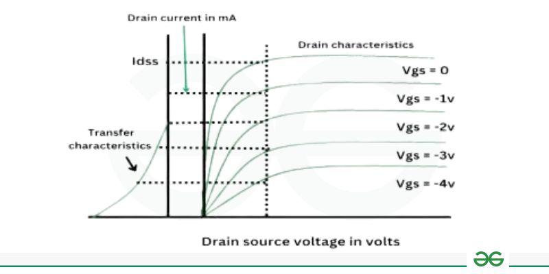
Transfer characteristics of JFET
Advantages of Junction Field Effect Transistor (JFET)
Modern technology depends upon transistors for their wide range of advantages, which are listed below:
- Stability: It offers good stability in various operating conditions.
- Low power consumption: it consumes little power, which makes it energy efficient.
- High impedance: JFETs have a high input impedance; these high input impedances can be well suited for amplifier circuits.
- Simplicity: JFETs are relatively simple to use and do not require the complex biassing arrangements often found in other transistors.
- No Gate Current: JFETs have no gate current flow, which simplifies circuit design in applications where current flow must be avoided.
Disadvantages of Junction Field Effect Transistor (JFET)
Though transistors are widely used, they still face some drawbacks, which are listed below:
- Unipolar Device: JFETs are unipolar devices, because the current flow can be controls through the movement of only one type of charge carrier (either electrons or holes).
- Gate-Source Leakage: JFETs can exhibit gate-source leakage currents, which is required in strict leakage current applications.
- Limited Availability: The availability is less, finding specific JFETs with specific characteristics can be challenging
- Low gain: it has low gain as compared to other types of transistors and cannot be used in high-gain applications.
- Cost: It is expensive, which can impact the overall cost of electronic devices.
Applications of Junction Field Effect Transistor
- Low-Noise Amplifiers: JFETs are ideal for low-noise amplifier applications in high-frequency signal processing, and audio circuits.
- High-Impedance Preamplifiers: JFETs are used in preamplifiers for high-impedance sensors, such as piezoelectric accelerometers and certain types of microphones, to maintain signal integrity.
- Switching Circuits: JFETs can be used as electronic switches in low-power and high-frequency applications where fast switching is required, such as in RF switching circuits.
- Sample and Hold circuits: In sample-and-hold circuits, JFETs can sample the input signal and hold its value until the next sampling period.
- Voltage Regulators: JFETs can also be used in voltage regulators to maintain stable output.
- Oscillators: JFETs are important in making oscillators that create repeating waveforms. They can also control the frequency, to generate stable waveforms.
Conclusion
Transistors are the basic building blocks of electronics, and there are a number of types that can be tailored to individual applications. JFETs are essential for the control of electrical circuits’ current and voltage, allowing a wide variety of applications. JFETs are known for their simplicity and are used in high-impedance applications for various purposes and operations. There’s also a lot of other transistors, but only JFETs are capable of showing very high impedance. Finally, in a wide range of electronic devices, transistors play an important role in amplifying signals, switching digital states, and controlling power. Factors such as voltage, current, frequency, and impedance need to be taken into account when selecting the type of transistor. Electronic engineers and enthusiasts alike must be able to understand the characteristics and uses of different types of transistors, so as to enable innovation and technological progress.
FAQs on JFET
How do JFETs act as voltage-controlled resistors?
JFETs can vary their resistance by adjusting the voltage applied to the gate terminal.
What is the drain current in JFET?
Drain current IDSS is the maximum current that flows between the drain and source terminals when the gate-source voltage is zero.
What is the main difference between N-channel JFET and P-channel JFET?
The majority carriers of N-channel JFETs are electrons, while in the P channel, the majority carriers are holes.
Share your thoughts in the comments
Please Login to comment...