Field Effect Transistor (FET) is a crucial electronic component. We are surrounded by numerous electronic devices all around, and now everything is just a click away from us. We went from desktop computers to supercomputers as technology advanced, and during this long journey, a transistor, an electronic component, played a significant role in this evolution. As of now, field-effect transistors, or FET transistors, are widely used transistors, providing the main active component in many integrated circuits. It has several advantages – less power consumption, and high input impedance, which is used in many devices to operate. In this article, we will study in detail about FET Transistor.
Field-Effect Transistor (FET) is a semiconductor device that consists of a channel made of a semiconductor material, with two electrodes connected at either end, namely the drain and the source.
What is FET?
FET is a type of semiconductor device which is having a semiconductor-based channel connected to two electrodes. The two electrodes named the drain and the source connected to either end. It has a third electrode named the gate which controls the current flow between the given two electrodes named the drain and the source.
The FET is classified into two types based on its mode of operation, specifically the enhancement mode and depletion mode FETs, depending upon whether the voltage applied at the gate terminal then increases or decreases the current flow through the channel. The idea of the field effect transistor depends on the possibility that a charge on a nearby thing can draw in charges inside a semiconductor channel. It essentially works by using an electric field effect, and this is how its name started.
Working of FET Transistor
It has 3 terminals: gate, drain, and source. The working principle is as per the following:
To allow electrons or holes to flow between the source and drain terminals, they are doped with material of the n-type or p-type variety.
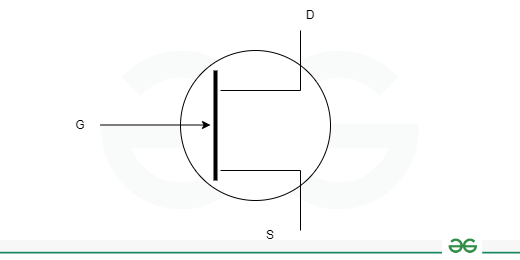
FET Symbol
An electric field is created in the channel area between the source and drain when a voltage is applied to the gate terminal. This electric field modulates the conductivity of the channel, behaving like a “valve” that controls the current flow between the source and drain. For an n-channel FET, applying a positive voltage to the gate attracts free electrons into the channel, increasing its conductivity and allowing more current to flow between the source and drain. For a p-channel FET, a negative voltage on the gate repulses holes, expanding conductivity.
By changing the gate voltage, the conductivity and current flow through the channel can be finely controlled. This permits FETs to be utilized as electronic switches and in amplifying circuits. The electric field effect gives a high input impedance and low noise performance, making FETs valuable in RF applications and as sensitive analog signal amplifiers.
Types of FET Transistor
A Field Effect Transistor (FET) operation depends on a controlled input voltage. By appearance, JFET and bipolar transistors are basically the same. BJT is a current-controlled device, and JFET is controlled by the input voltage. Two types of FETs are available.
- Junction Field Effect Transistor (JFET)
- Metal Oxide Semiconductor FET (MOSFET)
Junction Field Effect Transistor (JFET)
Junction Field Effect Transistors, or JFETs, operate based on the movement of electrons or holes, which are the majority carriers. These transistors are constructed using a silicon bar that contains PN junctions on its sides. To better understand JFETs, here are some essential points to keep in mind.
The gate of a JFET is formed by heavily doping the two sides of the N-type bar using diffusion or alloying techniques. These doped regions are known as the gate (G). The majority of carriers enter the semiconductor bar through the source, which serves as the entry point. On the other hand, the drain acts as the exit point, allowing the majority of carriers to leave the semiconductor bar. The channel refers to the N-type material area that facilitates the flow of majority carriers from the source to the drain. In the realm of semiconductor devices, there are two commonly used types of JFETs: N-channel JFET and P-channel JFET. Both variants play a crucial role in various electronic applications.
Output Characteristics of JFET:
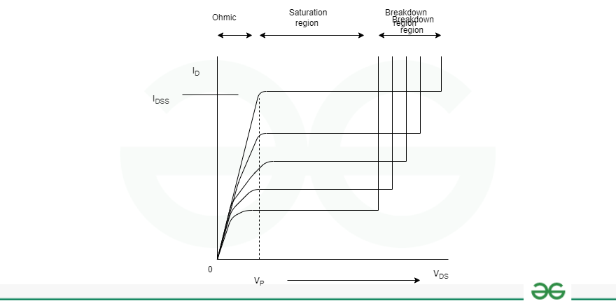
The output characteristics of JFET are drawn between drain current (ID) and drain source voltage (VDS) at constant gate source voltage (VGS), as shown in the following figure.
Initially, the drain current (ID) rises rapidly with drain source voltage (VDS), however, at a voltage known as pinch-off voltage (VP). Above the pinch-off voltage, the channel width turns out to be restricted to such an extent that it allows a very small drain current to go through it. Subsequently, drain current (ID) remains constant above the pinch-off voltage.
The main parameters of JFET are:
- AC drain resistance (Rd)
- Transconductance
- Amplification factor
AC drain resistance (Rd): is the ratio of the change in the drain source voltage (ΔVDS) to the change in drain current (ΔID) at a constant gate source voltage. It can be expressed as,
Rd = (ΔVDS)/(ΔID) at constant VGS
Transconductance (gfs): − It is the ratio of the change in drain current (ΔID) to the change in gate source voltage (ΔVGS) at a constant drain source voltage. It can be expressed as,
gfs = (ΔID)/(ΔVGS) at constant VDS
Amplification Factor (u) − It is the proportion of progress in channel source voltage (ΔVDS) to the change in gate source voltage (ΔVGS) constant drain current (ΔID).
It can be expressed as
u = (VDS)/(VGS) at constant ID
Biasing of JFET
There are two methods in use for biasing the JFET:
- Self-Bias Method
- Potential Divider Method or Voltage Divider Method
Self-Bias Method: The following figure shows the self-bias method for n-channel JFET. The drain current flows through Rs and produces the required bias voltage. Therefore, Rs acts as the bias resistor.
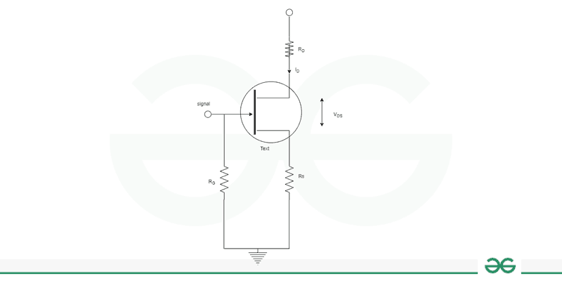
Self Bias Method
Hence, voltage across the bias resistor,
Vs = IDRS
As we know, gate current is negligible; the gate terminal is at DC ground, VG = 0.
VGS = VG – Vs = 0 – IDRS
VGS = – IDRS
VGS keeps the gate negative with respect to the source.
Voltage Divider Method: The following figure shows the voltage-divider method for biasing the JFETs. Here, resistors R1 and R2 form a voltage divider circuit across drain supply voltage (VDD), and it is more or less identical to the one used in transistor biasing.
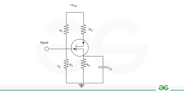
Voltage Divider Method
The voltage across R2 provides the necessary bias.
V2 = VG = VDD (R1 + R2 ) / R2
= V2 + VGS + ID + RS
Or VGS = V2 – IDRS
The circuit is designed so that VGS is always negative. The following formula can be used to determine the operating point:
ID = (V2 – VGS ) / RS,
and
VDS = VDD – ID(RD + RS).
Metal-oxide semiconductor field-effect transistors, or MOSFETs, are a new addition to the FET family with increased significance. It has a lightly doped P-type substrate into which two exceptionally doped N-type zones are diffused. A one-of-a kind component of this device is its gate construction. The channel is completely insulated from the gate. At the point when voltage is applied to the gate, it will develop an electrostatic charge.
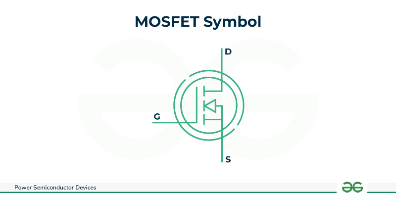
MOSFET Symbol
The terminology used for signifying the three essential FET configurations indicates the FET electrode that is common to both input and output circuits. This gives rise to the three terms: a common gate, a common drain, and a common source. The three different FET circuit configurations are:
- Common source: This FET configuration is probably the most commonly used. The common source circuit has medium input and output impedance levels. Both current and voltage gain can be described as medium; however, the result is the inverse of the input, for example, a 180° phase change. This provides good performance, and as such, it is in many cases considered the most widely used configuration.
- Common drain: This FET configuration is also called the source follower. The reason behind this is that the source voltage follows that of the gate. Offering a high input impedance and a low output impedance, it is generally used as a buffer.
- Common gate: This transistor provides a low input impedance while offering a high output impedance. Although the voltage is high, the current gain is low, and the overall power gain is also low when compared with the other FET circuit configurations available.
The common gate FET configuration provides a low input impedance while offering a high output impedance. As the gate is grounded, this acts as a barrier between input and output, giving a high level of isolation and preventing feedback, particularly at high frequencies. The voltage gain is high, the current gain is low, and the general power gain is low when compared with the other FET circuit configurations available. The other feature of this configuration is that input and output are in phase.
No current is permitted to flow in the gate region of the device. Also, the gate is an area of the device that is covered with metal. For the most part, silicon dioxide is used as an insulating material between the gate and the channel. Because of this, it is also called an insulated gate FET. There are two types of MOSFETs widely used:
- Depletion MOSFET
- Enhancement MOSFET
Depletion MOSFET
The following figures show the n-channel D-MOSFET and the symbol. The electric field of the capacitor changes when the gate voltage changes, which changes the n-channel’s resistance. In this case, we can either apply positive voltage or negative voltage to the gate. Depletion mode is the operation of a MOSFET with a negative gate voltage, while enhancement mode is the operation of a MOSFET with a positive gate voltage.
Most electrons are available on the gate, as the gate is negative, and it repels the electrons in the n channel. This activity leaves positive particles in the channel. In other words, a portion of the free electrons in the n channel are depleted. Accordingly, a smaller number of electrons are available for current conduction through the n channel. The more prominent the negative voltage at the gate, the less the current from the source to the drain. In this way, we can change the resistance of the n channel and the current from the source to the drain by varying the negative voltage on the gate.
Enhancement Mode
The following figure shows the n-channel D MOSFET under enhancement mode of operation. Here, the gate acts as a capacitor. However, the gate is open in this case. The number of electrons in the n channel increases as a result of this provocation. A positive gate voltage enhances or increases the conductivity of the channel. The larger the positive voltage on the gate, the greater the conduction from the source to the drain. Subsequently, we can change the resistance of the n channel and the current from the source to the drain by shifting the positive voltage on the gate.
FET Amplifiers
- FET (Common Source Amplifier Circuit): The common source FET configuration is the most commonly used of all the FET circuit configurations for many applications, providing a high level of all-round performance. The common source circuit has medium input and output impedance levels. Both current and voltage gain can be described as medium; however, the output is the inverse of the input, for example, a 180° stage change. This gives an overall performance, and as such, it is often considered the most widely used configuration.
- FET (Common Source Amplifier Circuit): The input signal enters by C. The gate is not affected by any DC voltage generated by the previous stages by this capacitor. The resistor R1 holds the door at ground potential. The T value could typically be associated with 1 Mω. The resistor R2 develops a voltage across it, holding the source over the ground potential. C2 acts as a bypass capacitor to provide additional gain at AC. The resistor R3 develops the output voltage across it, and C3 couples the AC to the next stage while blocking the DC.
- FET Common drain/source follower amplifier circuit: Like the transistor emitter follower, the FET source follower configuration itself gives a high level of buffering and a high input impedance. Because it is a field-effect device, the FET itself has a very high actual input resistance. This implies that the source follower circuit can provide superb performance as a buffer. The voltage gain is unity, but the current gain is high. The input and output are in phase. The circuit shown below gives a typical example of a FET source follower/buffer circuit. The capacitors C1 and C2 are used to couple the AC signal among stages and block the DC elements. The resistor R1 gives the gate bias, holding the gate at ground potential. The source circuit shows the resistor R2 to ground; its value is determined by the channel current that is required. The source follower circuit presents a very high impedance compared to the previous stage, and hence, the source follower is an ideal format for use as a buffer.
- FET (Common Gate Amplifier Circuit): The FET common gate amplifier circuit is the least widely used; however, it has a few characteristics that can be effectively used in certain applications. As such, the FET common gate circuit is seen as being used in a limited number of applications, although the common source and common drain configurations are used far more widely.
Characteristics of FET
Field Effect A transistor is a unipolar device where the current is carried only by the majority of part carriers (either by holes or electrons). A FET is a voltage-controlled device; by controlling the voltage between the gate and source, the output current gets varied.
Let us consider N-channel JFET for understanding the operating regions. The operation or characteristics of JFET are divided into three different regions: the ohmic region, the saturation region, and the cutoff region. The voltage that is applied to the drain is referred to as VDS (sometimes also as VDD), and the voltage that is applied to the gate is referred to as VGS or VGG.
Characteristics of Field-Effect Transistors (FET)
Ohmic Region
This prevents the channel from being pinched off and causes the current ID to rise because the VDS value is greater than zero and lower than VP. At the point when we increase the gate source voltage (VGS), the channel conductance falls and the resistance is increased. In this way, the depletion regions will spread more, creating a narrow channel. The channel resistance changes by and large from 100 ohms to 10K ohms and controls the voltage. Thus, transistors act as voltage-controlled resistors in this region.
Saturation Region (VDS > VGS-VP )
This region starts from where VDS is greater than VGS minus VP; here VP is the pinch-off voltage. Around here, the drain current ID completely depends on the VGS and is not an element of the VDS. The FET operates in this region to amplify the signal with respect to switching operations as well. From the figure, it is seen that when VGS is zero, the maximum current ID flows. The drain current decreases when the VGS is made more negative. At a specific value of VGS, the drain current flows constantly through the device. Consequently, this region is also called the constant current region.
Cutoff Region (VGS < VP)
The region in which the drain current ID is zero and the device is off is known as the cutoff region (VGS < VP). The gate source voltage VGS is less than the pinch-off voltage VP. This implies the value of VGS is more negative than VP. As a result, the channel closes, preventing the device from receiving any current.
Breakdown Region
This is the last and terminal region of the characteristics curve for the field effect transistor; you can see this region on the right corner. At this point, the voltage shown by the VDS between the drain and source is very high. The voltage is sufficiently high that the conductive channel is broken, and maximum current goes through the channel into the drain.
FET switching circuits
From the above discussion, the FET can be used as a switch by operating it in two regions: the cutoff region and the saturation region. At the point when the VGS is zero, the FET works in the saturation region, and maximum current flows through it. Consequently, it is like a fully turned-on condition. Similarly, when the VGS applied is more negative than the pinch-off voltage, the FET works in the cutoff region and does not allow any current to flow through the device. Consequently FET is in completely OFF condition. The FET can be used as a switch in different configurations; a portion of these are given below.:
- FET as a Shunt Switch
- FET as a Series Switch
FET as a Shunt Switch
At the point when the VGS applied is zero, the FET is turned on by operating in the saturation region, and its resistance is very small, 100 ohms. The output voltage across the FET is VOUT = Vin * {RDS/(RD + RDS (ON))}. The output voltage is considered zero due to the large resistance RD.
At the point when we apply the negative voltage, which is equivalent to the pinch-off voltage at the gate, the FET operates in the cutoff region and acts as a high-resistance device, and the output voltage is equivalent to the input voltage.
FET as a Series Switch
A FET acts as a series switch in this circuit. It acts as a closed switch if the control voltage is zero and an open switch if the control voltage is negative. At the point when the FET is ON, the input signal will show up at the output, and when it is OFF, the output is zero.
Applications of the FET
- Due to their low noise and high input impedance, amplifiers are utilized in multi-stage amplifiers as preamplifiers, buffers, and stages.
- Power control: Power MOSFETs are used in power control applications as switches because of their high productivity, low obstruction, and fast exchanging. utilized in drivers, power executives, and power supplies.
- Changes have the capacity to work as electronic switches by directing current stream with a little entryway voltage. It is utilized in computerized power supplies and RF circuits.
- Sensor connection points are utilized as info stages for sensors due to their high info impedance. Connect with sensors for light, pH, pressure, and different sensors.
- Oscillators are utilized as dynamic parts in oscillator circuits as a result of their low contortion and wide recurrence range
- RF circuits are utilized as intensifiers and blenders due to their high information impedance, low commotion, and ability to work at high frequencies.
- Logic systems: Because of their lower power utilization, higher rates, and capacity to work at lower voltages, rationale circuits are progressively supplanting BJTs.
- Simple circuits are utilized in simple circuits due to their great linearity and low commotion in circuits like activity amps, channels, and regulators.
Comparison between FET and BJT
|
BJT
|
FET
|
|
BJT has a three terminals they are emitter, collector and base
|
FET has a three terminals they are source, gate and drain
|
|
BJT has a low input impedance
|
FET has a high input impedance
|
|
BJT has a higher gain bandwidth product
|
FET has a lower gain bandwidth product
|
|
BJT has a higher voltage drop
|
FET has a lower voltage drop
|
|
BJT has a bigger size
|
FET has a smaller size
|
Conclusion
In conclusion, the Field Effect Semiconductor (FET) is a basic part of electrical designing because of its flexibility and viability across many applications. Its capacity to control the progression of current in light of an applied voltage, joined with properties like high info impedance and low power utilization, makes it a fundamental primary part in present day hardware. FETs are generally utilized in computerized circuits, speakers, exchanging power supply, and memory gadgets, framing the underpinning of electronic plan. The two fundamental assortments, Intersection Field Effect Semiconductor (JFET) and Metal-Oxide-Semiconductor FETs (MOSFET), each enjoy benefits that add to the range of uses.
FAQs on FET Transistor
How really does bias influence the activity of a field-effect semiconductor?
Biasing ensures that the FET works in the ideal district — ON or OFF — by setting out the fitting voltage at the entryway terminal corresponding to the source.
What are the principal benefits of utilizing FETs in amplifier circuits?
FETs have a high information impedance, low commotion, and proficient sign intensification, making them ideal for an assortment of speaker applications.
What are the most well known utilizes for CMOS circuits that utilization both N-Channel and P-Channel FETs?
Due to their low power utilization and extraordinary upheaval obstruction, CMOS circuits are generally utilized in modern coordinated circuits, computer chips, and memory gadgets.
In a FET, what is the primary function of the gate terminal?
The gate terminal of a FET directs the progression of flow between the source and channel terminals by changing the electric field inside the semiconductor.
How is a N-channel FET not the same as a P-channel FET?
N-channel FETs lead when a positive voltage is applied to the door, yet P-channel FETs direct when a negative voltage is applied.
Share your thoughts in the comments
Please Login to comment...