The Schottky diode is popularly known as a hot-carrier diode, low-voltage diode, or Schottky barrier diode. It is a type of diode formed by the junction of a semiconductor with a metal. We know that in a PN junction diode, p-type and n-type semiconductors are joined collectively to form a PN junction. To the contrary, a Schottky diode replaces the p-type semiconductor with metals like aluminium.
Schottky diode has multiple characteristics which makes it a better choice over other diodes in the electronic industry. It displays characteristics like fast switching action and a low forward voltage drop. The symbolic representation of this diode, the construction of this diode, the energy band of the diode and what the V-I characteristic graph of this diode looks like.
What is Schottky Diode?
A Schottky diode is a type of diode with a metal-semiconductor junction instead of the typical semiconductor-semiconductor junction found in standard diodes. The Schottky diode has characteristics such as Low Forward Voltage Drop, Fast Switching Speed and other unique features that make it more suitable for various applications such as rectification, voltage clamping, voltage regulation, and RF detection.
Symbol of Schottky Diode
The symbol for a Schottky diode in an electronic circuit diagram is similar to that of a standard diode but with a few distinguishing features.

Symbol of Schottky Diode
The arrowhead points towards the cathode (K), which is the side with the metal contact. The horizontal line at the cathode side is shorter than the anode side, indicating the metal-semiconductor junction.
Schottky Diode Construction
We know that unlike a normal P-N junction diode ,a Schottky diode is equipped with a metallic contact. On further analysis the construction of the diode is like:
- Schottky diodes are constructed using semiconductor materials. Silicon (Si) is a common choice, although other materials can also be used.
- The differentiating feature in Schottky diode is the metal-to-semiconductor junction. A metal contact (made of metals like Pt, W, Al) is directly connected to the semiconductor material (usually n-type silicon).
- The region beneath the metal contact is n-type semiconductor. It has a higher concentration of electrons (i.e, electrons are the majority charge carriers).
- Schottky diodes have a depletion region near the junction. Since we do not have a p-type region, this depletion region is much thinner than a normal diode.
- The interaction of electrons from the n-type semiconductor with metal atoms is the major driving factor for formation of this region.
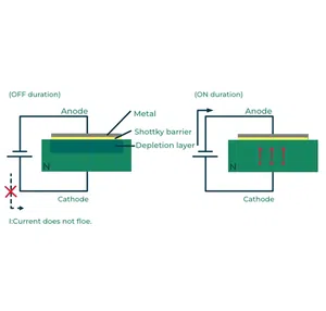
Working Of Schottky Diode
Given Below is the diagram of Schottky diode

Schottky Diode
A Schottky diode is formed by joining a metal (commonly aluminum or platinum) with a semiconductor material (usually silicon or gallium arsenide) to create a metal-semiconductor junction.
- When the metal comes in contact with the semiconductor, a potential barrier, known as the Schottky barrier, is created at the junction due to the difference in work functions between the metal and semiconductor. This barrier prevents the flow of electrons from the metal into the semiconductor.
- When a forward bias voltage is applied across the Schottky diode (anode connected to the metal side, cathode connected to the semiconductor side), the applied voltage reduces the height of the Schottky barrier.
- The lowered barrier allows electrons to easily flow from the metal into the semiconductor, resulting in a low forward voltage drop (typically 0.2 to 0.4 volts for silicon Schottky diodes). This characteristic minimizes power dissipation and makes the diode suitable for low-voltage applications.
- Schottky diodes exhibit very fast switching action due to the absence of a depletion region, which is present in traditional PN junction diodes. This makes them ideal for high-frequency applications where rapid switching is required.
- In the reverse bias condition (positive voltage on the semiconductor side, negative voltage on the metal side), the Schottky diode exhibits a small reverse leakage current due to thermionic emission of electrons over the lowered Schottky barrier.
- Unlike PN junction diodes, Schottky diodes have virtually no reverse recovery time. This means there is no delay when transitioning from the conducting to non-conducting state, making them suitable for high-frequency rectification.
V-I Characteristic of Schottky Diode
Given below is the V-I characteristics of Schottky diode

V-I characteristics of Schottky diode
The V-I characteristics of Schottky diodes are very much similar to the PN junction diode. Current is the dependent variable while voltage is the independent variable in the Schottky diode.
Forward Bias (F): When a forward bias voltage is applied across a Schottky diode (positive voltage on the anode, negative voltage on the cathode), the V-I characteristics show that it conducts current very quickly with a relatively low forward voltage drop. This rapid conduction is due to the low Schottky barrier at the metal-semiconductor junction. The forward current increases exponentially with voltage, similar to a standard diode.
Reverse Bias (R): In the reverse bias condition (positive voltage on the cathode, negative voltage on the anode), the V-I characteristics of a Schottky diode display a small reverse current, often referred to as the leakage current. This reverse current is typically larger than that of a silicon PN junction diode because of the absence of the depletion region found in PN junctions. However, it is still relatively low compared to other diode types.
Breakdown Voltage: Schottky diodes do not exhibit a well-defined breakdown voltage like some other diode types. Instead, they have a reverse breakdown mechanism known as “avalanche breakdown.” When the reverse voltage exceeds a certain level, the diode can experience avalanche breakdown, leading to a sudden increase in reverse current.
Cut-in Voltage: The cut-in voltage (also called the knee voltage) for a Schottky diode is typically very close to zero volts, which means it starts conducting at very low forward bias voltages.
Energy Band Diagram
The energy band diagram of a Schottky diode is a graphical representation of the energy levels of device demonstrating the electrons and holes behaviour at the metal-semiconductor junction. It shows variation of energy with distance x from junction.

Energy Band Diagram
Here’s an explanation of the energy band diagram of a Schottky diode:
The left side in diagram represents the metal contact. The Fermi level in metals is relatively high and close to the conduction band. The high Fermi level indicates that there are plenty of free electrons available in the metal.
The right side of the diagram represents semiconductor material( n-type silicon for Schottky diodes). The semiconductor consist of the valence band (Vb), the conduction band (Cb), and the intrinsic energy gap (Eg). Due to excess of electrons in n-type silicon, the Fermi level is closer to the conduction band.
The energy difference between metal and semiconductor creates a region at the metal-semiconductor interface called the Schottky barrier. The difference between levels i.e the barrier height is for electrons to move from the metal into the semiconductor.
In forward bias condition, electrons from the metal gain enough energy to overcome the Schottky barrier and move into the semiconductor’s conduction band. This results in the flow of current from the metal to the semiconductor. The barrier height prevents reverse current flow, resulting in rectification and the characteristic behaviour of a Schottky diode.
Schottky Barrier
Schottky barrier in different states
The energy difference between metal and semiconductor creates a region at the metal-semiconductor interface called the Schottky barrier. It is an electrical junction characterized by the presence of a barrier to the flow of electric charge carriers (electrons and holes) at this junction.
The Schottky barrier acts as a valve for electrons. When you apply voltage in one direction (forward bias), current flows easily through the wire to the electronic device, and that’s over for now. But when you apply the voltage in the opposite direction (reverse bias), the barrier will be higher and block the flow of electrons.
In forward bias the Schottky barrier has a low voltage drop, which means it conducts current with less current. Loss of energy. This is one of its advantages in electronic circuits.
Schottky Clamped Transistor

Clamped Transistor
Clamping means to maintain the voltage limits i.e. shifting input signal to a particular value by manipulating input characteristics.
In order to make a Schottky-clamped transistor, we add a Schottky diode in parallel with the base-emitter junction of the transistor. This results in a specialized type of bipolar transistor .
The benefit we get from this design is improved switching speed and efficiency of the transistor. On careful observation we can see that this diode is connected in such a way that it forms a low-resistance path for the base current i.e. this path offers very less resistance to the flowing current.
The Schottky diode provides a low forward voltage drop and fast switching characteristics. In forward mode, the Schottky diode effectively clamps the voltage across the base-emitter junction to a lower value than in standard bipolar transistors. This results in a reduced storage time and the switching off speed of the transistor is increased.
This design is majorly used in applications that require rapid switching , such as RF amplifiers and high-speed digital electronics.
Schottky Diodes in Logic Gates
The Schottky are used in logic gates due to their unique characteristics
- AND Gates: Schottky diodes are used to perform AND operation by connecting the inputs to the anodes of the diodes and the output to the cathode of the diodes.
- OR Gates: Schottky diodes are used to perform OR gate configurations by connecting the cathodes of the diodes and the output is connected to the anode of the diodes
- Inverter Gates: Schottky diodes can be used for inversion of the input signal by connecting the input to the cathode of the diode and the output to the anode.
Characteristics of Schottky Diode
- Low Turn-On voltage: The voltage required to turn on a Schottky diode is comparatively low as compared to other diodes.
- Low Forward Voltage Drop: Due to this property of diode it finds its application in Power Circuits because it is well adapted due to low voltage drop. This property also makes them best devices to be used in Power Rectifier Applications with high current density.
- Fast Recovery Time: Due to the semiconductor contact , Schottky diodes show a very fast recovery time making the circuits very fast. Thereby these diodes are used in Fast-Clamp Diode Applications where base junction is forward biased.
- Low Loss Energy: Schottky diode shows a very low energy loss even at higher frequencies. Due to this Schottky diodes are generally used in Solar Cells. Solar cells generally store energy and Schottky diodes prevents them from discharging.
Difference between Schottky and P-N junction Diode
These differences highlight the distinct characteristics and applications of PN junction diodes and Schottky diodes in electronic circuits.
|
Parameter
|
P-N Junction Diode
|
Schottky Diode
|
|
Construction
|
Consists of p-type and n-type semiconductor regions forming a PN junction.
|
Consists of a metal-semiconductor junction with a metal (e.g., aluminum) and a semiconductor (e.g., silicon).
|
|
Forward Voltage Drop (Vf)
|
Higher forward voltage drop (typically 0.6 to 0.7 volts for silicon diodes).
|
Lower forward voltage drop (typically 0.2 to 0.4 volts for silicon Schottky diodes).
|
|
Switching Speed
|
Slower switching speed due to the presence of the depletion region.
|
Faster switching speed due to the absence of a depletion region.
|
|
Reverse Leakage Current
|
Lower reverse leakage current (in the nA range for silicon diodes).
|
Higher reverse leakage current (typically in the μA range for silicon Schottky diodes).
|
|
Type Of Device
|
It is a bipolar device
|
It is a unipolar device
|
Applications of Schottky Diode
Some common applications of Schottky diode include:
- Power rectifier: When having high power supply, Schottky diode acts as a rectifier. The high current density and low voltage drop shows that the wastage of power is lesser than the normal PN junction diodes which makes them more efficient.
- RF mixer: Schottky diodes are widely used in RF and microwave circuits due to their fast switching speed and low noise characteristics. They can be used as detectors, mixers, and frequency multipliers in these circuits.
- Electronic appliances: Schottky diodes finds its use in logic gates, digital circuits, and memory devices. Their low forward voltage drop and high efficiency makes them ideal for applications such as voltage regulators and DC-DC converters.
- They are used in Battery charging circuit, Switching power supplies, LED drivers, Audio amplifiers, Voltage clamps.
- Power OR circuits: Schottky diodes are used in power ORing circuits to select between multiple power sources, minimize voltage drops, provide fast response times, and prevent reverse current flow, improving system reliability and efficiency.
- Solar Cell Applications: Schottky diodes in solar cell systems prevent reverse current flow, optimize power extraction, regulate charging, and enhance overall efficiency and reliability.
Advantages of Schottky Diode
Advantages of Schottky diodes are
- Low Forward Voltage Drop: Schottky diodes have a lower forward voltage drop compared to standard silicon diodes.
- Fast Switching Speed: Schottky diodes has fast switching speeds which makes them ideal for high-frequency applications.
- Negligible Reverse Recovery Time: Schottky diodes have no reverse recovery time that eliminates the delay between the end of the reverse voltage and the return of the diode to a non-conducting state.
- High Temperature Operation: Schottky can work on high temperature which make them suitable for high temperature environment.
Disadvantages of Schottky Diode
Disadvantages of Schottky diodes are
- Temperature Sensitivity: The forward voltage drop of Schottky diodes is more temperature-sensitive compared to p-n junction diodes. As the temperature increases, the forward voltage drop also increases, which can affect the diode’s performance in high-temperature environments.
- Lower Reverse Recovery Time: While the lower reverse recovery time of Schottky diodes is an advantage for fast-switching applications, it can be a disadvantage in some cases. In certain applications where a slight delay is needed between switching states, Schottky diodes may not be suitable.
- High Reverse Leakage Current: Schottky diodes tend to have higher reverse leakage current compared to standard p-n junction diodes. This can result in increased power consumption and reduced performance in low-power applications.
- Noise Generation: Schottky diodes can generate more electrical noise compared to some other diode types, which can be a concern in sensitive analog circuits.
- Higher Cost: Schottky diodes are often more expensive to manufacture compared to standard p-n junction diodes due to the specialized metal-semiconductor junction.
Conclusion
In the end we can say that Schottky diode is a diode formed by the junction of semiconductor with a metal. The ‘fast-switching action’ property of this diode is a vital characteristic which makes Schottky diode a major device in fast-clamp switching circuits. An efficient channelization of this diode has been seen in the industry of electronics. The diode is comparatively smaller than other diodes but generally gives better performance than other diodes due to its ability to provide multiple power supplies.
Schottky Diode – FAQs
Why can Schottky diodes be switched off much faster than the p-n junction diode?
Due to the metal-silicon junction charges do not get stored, due to this there is no reverse recovery time and switching is faster.
What is meant by reverse-recovery time?
If a diode is initially driven in forward bias and the polarity suddenly switches to reverse bias, the diode will still remain conducting for some time. The time required for conduction to settle into the reverse bias state is the diode’s reverse recovery time.
What are the disadvantages of Schottky Diode?
These diodes can’t withstand much higher voltage without break down thereby causing excessive heating. They are even more costly.
What are the other types of diodes?
Some other types of diodes are P-N Junction Diode, Small Signal Diode, Rectifier Diode, Light Emitting Diode (LED), Photodiode, Laser Diode, Tunnel Diode, Zener Diode.
Share your thoughts in the comments
Please Login to comment...