IGBT stands for Insulated Gate Bipolar Transistor. IGBTs find extensive applications in various domains, including household appliances like air conditioners and refrigerators, industrial motors, and automotive main motor controllers. Their utilization of these devices serves to enhance overall energy efficiency. IGBT is also called insulated gates because of the insulated gates the IGFETs have high current gain.
What is an Insulated Gate Bipolar Transistor?
IGBT, or Insulated Gate Bipolar Transistor, represents a significant advancement in power electronics and a bipolar transistor with an insulated gate terminal. It is a type of power transistor that integrates an input MOS (Metal-Oxide-Semiconductor) with an output bipolar transistor. It is a three-terminal power semiconductor device that forms an electronic switch. It is commonly employed as a switching device in inverter circuits, facilitating the conversion of DC (Direct Current) to AC (Alternating Current) power.
It combines the advantages of both MOSFET and BJT technologies and something comes good out of these two devices. MOSFETs are known for their high-speed switching capability and high input impedance, while BJT offers high current gain and low saturation voltage. The structure of an IGBT typically consists of a MOSFET-like gate, which controls the flow of current between the collector and emitter, and a BJT-like structure for amplifying the current.
This combination allows IGBT to handle high voltage and current levels while maintaining efficient switching. The symbol of an IGBT reflects its dual nature, with elements resembling both MOSFET and BJT symbols. It’s important to note that IGBT has largely replaced power BJT in many high-power applications due to its superior performance characteristics. IGBT offers the best of both the MOSFET and BJT worlds, making them a crucial component in various power electronic applications. Their ability to switch high currents efficiently while maintaining fast switching times has made them essential in modern electronics.

IGBT Symbol

Pin Diagram of IGBT
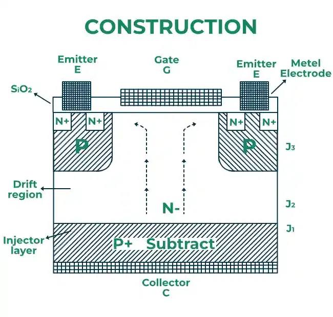
Construction of IGBT
The IGBT combines the input characteristics of a MOSFET with the output characteristics of a BJT, resembling the structure of an N-channel MOSFET and a PNP BJT in Darlington configuration. Additionally, the resistance of the drift region can be integrated. In terms of the IGBT’s structure, there are multiple current paths. The primary path is from the collector to the emitter, involving the sequence: “collector, P+ substrate, N-, P, emitter,” which aligns with the PNP transistor equivalent. There’s also a secondary path: “collector, P+ substrate, N-, P, N+, emitter,” which necessitates the inclusion of another NPN transistor, as illustrated in the figure below.
The IGBT consists of four semiconductor layers arranged to create a PNPN structure. The collector (C) electrode connects to the P layer, while the emitter (E) is positioned between the P and N layers. Construction employs a P+ substrate, with an N- layer atop it is forming PN junction J1. Two P regions are crafted on the N- layer, creating PN junction J2. The gate (G) electrode is positioned within a gap in the middle of the P region. Metal electrodes serve as the emitter and gate, with the emitter directly connected to the N+ region and the gate insulated by a silicon dioxide layer. The P+ layer, referred to as the injector layer, injects holes into the N- layer, while the N- layer itself is called the drift region, with its thickness proportional to voltage-blocking capacity.
The upper P layer is known as the body of the IGBT. The N- layer is designed to establish a current path between the emitter and collector, utilizing a channel formed beneath the influence of the voltage applied to the gate electrode. The N- layer is strategically designed to provide a path for the current to flow between the emitter and collector. This current path is influenced and controlled by the voltage applied to the gate electrode. By varying this voltage, the IGBT can regulate the flow of current through the device, making it an essential component in various power electronics applications.
Construction of IGBT
Working of IGBT
IGBT has three terminals collector (C), emitter (E) and gate (G). These terminals serve distinct roles in controlling current flow through the device, collector and emitter are related to the conductance path whereas the gate terminal is responsible for the controlling of the device and IGBT Operation. In the operation of an IGBT, the collector-emitter connection is established with the collector at a positive voltage compared to the emitter. These forward biases junction J1 and reverse biases junction J2.
Notably, there is no voltage applied to the gate at this stage. Due to the reverse bias at J2, the IGBT remains in the off state, preventing any current flow between the collector and emitter. When a positive gate voltage (VG) is applied relative to the emitter, negative charges accumulate beneath the SiO2 layer due to capacitance. As VG increases, more charges accumulate, forming a layer in the upper P-region when VG exceeds the threshold voltage.
This layer effectively creates an N-channel that connects the N- drift region and N+ region. Electrons from the emitter then flow from the N+ region into the N- drift region, while holes from the collector are injected from the P+ region into the N- drift region. The excess of both electrons and holes in the drift region enhances its conductivity, enabling current conduction. Consequently, the IGBT switches on and allows current to flow between the collector and emitter.
IGBT can be controlled or turn ON or OFF by simply activating deactivating the gate terminal. As the positive input voltage is applied then it will turn ON state and as the input voltage goes zero or negative then it will be turn OFF – also it has low channel resistance which results in the smooth flow of current in the device.
Parameters
There are some mathematical formulas of IGBT given below and these equations and parameters are fundamental for the analysis and design of circuits incorporating IGBTs.
- Collector Current (Ic): Collector current is the electric current flowing from the collector to the emitter of an IGBT. It can be determined using Ohm’s Law also. Here, Vce represents the collector-emitter voltage, and Rl is the load resistance.
Ic = Vce / Rl.
- Gate Current (Ig): Gate current is the current necessary to activate or deactivate the IGBT. It can be calculated using the gate voltage and gate-source capacitance (Cgs):
Ig = Cgs * dVgs/dt
where dVgs/dt is the change in gate-source voltage over time.
- Switching Losses (Ps): Switching losses in an IGBT result from energy dissipation during the turn-on and turn-off transitions. These losses are determined by the formula:
Ps = 0.5 * Vce * Ic * fsw * (Eon + Eoff)
where Vce is the collector-emitter voltage, Ic is the collector current, fsw is the switching frequency, and Eon and Eoff are the turn-on and turn-off energies.
- Forward Voltage Drop (Vf): The forward voltage drop is the voltage across the IGBT when it is in the conducting state and Vce(sat) represents the saturation voltage.
Vf = Vce + Vce(sat)
- Power Dissipation (Pd): It is calculated with the formula mentioned and here Vce is the collector-emitter voltage, and Ic is the collector current.
Pd = Vce * Ic
- Gate Charge (Qg): Gate charge is the total charge needed to transition the IGBT from off to on. It’s related to the gate current and gate-source voltage:
Qg = ∫(Ig dt)
where Ig is the gate current, and the integral is taken over the switching time.
- Junction Temperature (Tj): The junction temperature of the IGBT can be estimated considering power dissipation and thermal resistance. Here Ta is the ambient temperature, Pd is the power dissipation, and Rth is the thermal resistance.
Tj = Ta + (Pd * Rth)
IGBT Characteristics
Some of the characteristics followed up in IGBT are as follows:
- VI Characteristics of IGBT
- Transfer Characteristics of IGBT
- Switching Characteristics of IGBT
V-I Characteristics of IGBT
IGBT differ from BJT in that they are voltage-controlled devices requiring only a small gate voltage, VGE, to regulate collector current, IC. However, the gate-emitter voltage, VGE, must surpass the threshold voltage, VGET. The transfer characteristics of IGBT illustrate the relationship between input voltage, VGE, and output collector current, IC.
- When VGE is 0V, the device remains off with no IC, and when VGE slightly increases but stays below VGET, it remains off but may exhibit a leakage current.
- Once VGE surpasses the threshold, IC begins to rise, turning the device on. As a unidirectional device, current flows in only one direction.
- IGBT characteristic curves, as depicted in the provided graph, demonstrate the relationship between collector current, IC, and collector-emitter voltage, VCE, at different VGE levels.
- At VGE < VGET the GBT is in cutoff mode, resulting in IC = 0 at any VCE. Beyond VGE > VGET, the IGBT enters the active mode, where IC increases with rising VCE.
Moreover, for each VGE where VGE1 < VGE2 < VGE3, IC differs. It’s crucial not to exceed the reverse voltage or forward voltage beyond their respective breakdown limits, as this can lead to uncontrolled current flow.

VI-characteristics-of-IGBT
Transfer Characteristics
The transfer characteristics of IGBT shows the graph between the collector current and gate emitter voltage i.e. between the IC and VGE . The IGBT remains in the OFF state as the value of the gate emitter voltage is less than that of the threshold voltage :
VGE < VGET

Transfer Characteristics
Switching Characteristics
The switching characteristics of IGBT are shown below in the figure :
Here turn on time is of two components delay time and rise time and according to this delay time is the time required in rising of the collector current from ICE to 0.1 IC and fall in the collector emitter voltage from VCE to 0.9 VCE , and vice versa with the rise time that it is the time in which collector current rises to IC and collector voltage falls to 0.1 VCE .
t on = t dn + t r

Switching Characteristics of IGBT
Advantages
- Safe Operating device
- Cost efficient driver circuits.
- IGBTs are smaller in size, easy to handle.
- Highly efficient voltage controlled devices.
- Higher Output Impedance
- Low switching loss and power loss
- Less voltage drop
Disadvantages
- IGBTs cannot stop the flow of high reverse voltages. no secondary breakdown for these transistors.
- Cost effective
- Low switching speed when compared to other transistors.
- Low input impedance.
- Switching frequency of IGBTs up to 50KHz less than BJT and MOSFET.
Applications
IGBT find application in a wide range of uses, including:
- AC and DC motor drives
- Unregulated Power Supply (UPS)
- Switch Mode Power Supplies (SMPS)
- Traction motor control
- Induction heating
- Inverters
- They are designed to combine an isolated-gate FET for control input and a bipolar power transistor into a single device, enhancing versatility.
Conclusion
IGBT are essential in a wide range of applications due to their versatility. They perform critical functions like regulating voltage and current, controlling motors, powering devices, supporting renewable energy systems, and enabling electric vehicle propulsion systems. In the context of voltage and current regulation, IGBT are vital for ensuring a consistent and controlled supply of power. Their capability to handle high voltages and currents makes them well-suited for applications demanding precision, such as industrial automation and grid-connected systems.
Basically it is a switching device which is control like the MOSFET but it has the output characteristics similar to that of BJT. It is used in power amplifier and other switching devices and its operation is not so complex, just depends on the input terminal voltage to turn it ON and negative or zero input voltage to turn it OFF. IGBT is free from the second breakdown problem which usually occurs in the BJT.
IGBT – Frequently Asked Questions
What is the function of IGBT?
The primary purpose of an IGBT is to enable rapid switching of electrical currents, minimizing switching losses, as reflected in its name, “Insulated Gate Bipolar Transistor.”
What are the three terminals of IGBT ?
IGBT integrate a PNP transistor output with an insulated gate N-channel MOSFET output, forming transconductance modules featuring three essential terminals: the emitter, collector, and gate. The gate terminal governs the device, while the emitter and collector are connected to the current and the conductance path, respectively.
Is IGBT is a bipolar or unipolar ?
An IGBT is a bipolar device that uses both electrons and holes as carriers, thanks to its intricate design incorporating a MOSFET structure at the input stage and a bipolar output, enabling it to achieve a low saturation voltage while maintaining relatively fast performance.
What is the efficiency of IGBT ?
Hybrid IGBT are a great choice for these tasks because they fulfill important criteria like minimal switching loss, low VCE, high power conversion efficiency, and affordability. With an efficiency of over 97%, these options guarantee a broad operating frequency range when employed in car chargers.
Share your thoughts in the comments
Please Login to comment...