The term “transistor” originated in 1951 at Bell Laboratories by Dr. Shockley and associates. The transistor is a widely utilized essential component in modern electronic systems. Transistors generally come in two types. They are field effect transistor (FET) and BJT which is bipolar junction transistor. Signal amplification, or amplifier usage, is a common use of a BJT ( bipolar junction transistor), which is a three-terminal semiconductor device composed of combinations of p-type and n-type semiconductors. As we know this semiconductor device consists of the p-n junction and it is used or able to amplify the signal or magnify the signal. Through this the current flows and basically it contains silicon, they are also called bias resistor built-in transistors and their main objective is that -as the small current flows between the base and emitter which can control a large flow of current between the regions of collector and emitter terminals.
What is Bipolar Junction Transistor?
The concept of BJT refers to a three-terminal semiconductor device consisting of two p-n-junctions that are formed by sandwiching either p-type or n-type semiconductors between two p-type semiconductors. Transistors can be used to transfer input signals through the circuits having lower to higher resistance. A BJT may also be implemented as a true solid-state switch in electrical circuits and can also be used to increase the strength of a weak signal.

Symbol of BJT
Construction of BJT
Combinations of p-n junctions, or build a BJT i.e. a BJT is made of p and n type semiconductors. The two junctions divide the three semiconductors of a BJT which are: the base, collector, and the emitter. The emitter and collector part of transistor are placed on each side of the base.
- Emitter (E) : The outermost layer of a transistor, is commonly known as the emitter, it is heavily doped with N- type or P-type semiconductor material. P-type material is often employed to produce the emitter of a PNP transistor, whereas N-type material is mostly utilized for creating the emitter of a NPN transistor.
- Base (B): The intermediate layer is called the base, it forms a narrow zone between the emitter and collector and is slightly doped. Its made up of different material than the emitter. A NPN transistor’s base is P-type, while a PNP transistor’s base is of N-type.
- Collector (C): The inner layer is called as collector, and it has a modest doping level. The type of semiconductor used in the designing is the same as that of the emitter. An NPN transistor’s collector is formed from N-type material, whereas a PNP transistor’s collector is made of P-type material.
There are two junctions formed in BJT . They are –
- Emitter-Base junction: The Emitter-Base junction of a BJT refers to the junction that is formed between the emitter and base. During normal operation , this junction is forward-biased.
- Collector-Base junction : Collector-Base junction is the name given to the junction that is formed between the emitter and base. During normal operation , this junction is reverse-biased.

Construction of BJT
Operation of BJT
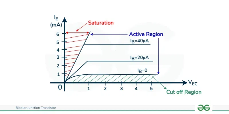
BJT operates in three regions:
- Active region: The transistor is on in this region. When the collector-base junction is reverse-biased while the emitter-base junction is in forward-bias, then BJT works in the active area. As a result, BJT is used as an amplifier. The collector current is proportional to and controlled by the base current and relatively insensitive to VCE. In this region the transistor can be an amplifier.
(IC = βIB)
- Saturation region: The saturation region arises when the collector-base junctions and the emitter-base junction are both forward-biased. The transistor is on. The collector current varies very little with a change in the base current in the saturation region. The VCE is small, a few tenths of a volt. The collector current is strongly dependent on VCE unlike in the active region. It is desirable to operate transistor switches in or near the saturation region when in their on state.
Ic = I(saturation)
- Cut-off region: Because the emitter and collector junctions are both in the reversed bias, so the BJT is off in this condition and vary small amount of current flows from collector to the emitter. There is no current between emitter and the collector.
(IB = 0 therefore IC = 0)

Regions of Operation of BJT
Types of BJTs
BJT could possibly be divided into two broad groups based on how the p-type and n-type semiconductor materials are arranged physically:
- PNP Bipolar Junction Transistor
- NPN Bipolar Junction Transistor
NPN Transistor
P-type material is sandwiched between the two n-type of semiconductors in NPN type semiconductor. The two semiconductors of the n type act as the emitter and collector, respectively, while of p-type acts as the base. The Emitter-base junction is forward bias and collector-base is reverse bias during the forward active state of NPN transistor. Only if voltage exceeds the barrier potential, which is 0.3 volts for germanium transistors and 0.7 volts for silicon transistors, is the emitter-base junction forward biased.
Due to forward bias on the emitter- base junction the free electrons move towards the base region in N –type emitter. This constitutes emitter current . Direction of conventional current is opposite to the flow of electrons. Electrons after reaching the base region tend to combine with the holes. If these free electron combine with holes in the base, they constitute base current .
Most of the free electrons do not combine with the holes in the base as base and the width is made extremely small and electrons do not get sufficient holes for recombination. Thus most of the electrons will diffuse to the collector region and constitutes collector current . There is another component of collector current due to the thermal generated carriers. known as reverse saturation current and is quite small.

NPN BJT
PNP Transistor
The two p-type of semiconductors are sandwiched between the n-type semiconductor in a PNP BJT. The two p-type semiconductors act as the emitter and collector, respectively, and the n-type acts as the base. In a PNP transistor, current is due to the movement of holes, as opposed to the mobility of free electrons in an NPN transistor. The collector base junction of a PNP transistor is reverse biased, whereas the emitter base junction is biased forward. The holes within the emitter area flow into the base region due to the forward bias at the emitter-base junction. This constitutes the emitter current .
The holes after reaching the base region, combine with the electrons in the base and constitutes base current. Most of the holes do not combine with the electrons in the base region as base width is made extremely small, and holes does not get sufficient electrons for recombination.
Thus most of the holes diffuse to the collector region and constitutes collector region. There is small component of collector current due to the thermally generated carriers . This is called reverse saturation current.

PNP BJT
The transistor is fundamentally a current-controlled device, hence the voltage between its terminals has significant effect on its behavior.
- Voltage Control: If we talk of input, the BJT is primarily a voltage-controlled device. The base-emitter junction voltage determines the current flows between the emitter and the collector. And the base-emitter junction voltage determines whether the transistor is “on” or “off” and hence influences the amount of current that may travel through it.
- Charge Control: The current between the collector and emitter is determined by the movement of charge carriers, such as electrons or holes, in the base area. Between the collector and emitter, a considerably bigger current is controlled by a much smaller current at the base. Holes are charge carriers in PNP transistors , whereas NPN transistors have electrons. The transistor’s ability to work as a switch or an amplifier are determined by the number of charge carriers delivered into the base region.
- Current Flow: The current that flows between the collector and emitter of a BJT is its main output. The voltage across the base-emitter junction controls base current, which influences the collector current. The transistor’s current gain, or β (beta), explains the relationship between IC, IB, and IE, where ,IC=collector current , IB=base current , and IE= emitter current (IE). The collector current should, in theory, be equal to β times the base current, or:
IC = β * IB.
Bipolar Transistor Configurations
There are basically three possible ways to connect BJT in an electric circuit are:
- Common Collector Configuration
- Common Base Configuration
- Common Emitter Configuration.
Common Base Configuration
The base of transistor is grounded in common base characteristics , with the emitter acting as the input and the collector as the output. The emitter-base junction is biased forward, whereas the junction between the collector and the base is reverse biased. Low voltage gain but high current gain is offered by the CB arrangement. It is frequently employed in impedance matching. It reverses the output signal’s phase with respect to the input and frequently utilized as a buffer between circuits with high and low impedance and in high-frequency applications like RF amplifiers.
Characteristics curves
There are two important characteristics of a transistor.
- Input characteristics- The curve drawn between emitter current and emitter – base voltage for a given value of collector – base voltage is known as input characteristics. Input characteristics of CB ΔVCB at constant:
Rin = ΔVBE/ΔIE

Input characteristics
- Output characteristics – The curve drawn between collector current and collector – base voltage, for a given value of emitter current is known as output characteristics. Output characteristics of CB ΔIE at constant:
Rout =ΔVCB /ΔIB
.png)
Output characteristics
Common Emitter Configuration
Emitter of transistor is grounded in common-emitter characteristics , and the base serves as input and the collector serves as output. The CE configuration is like the CB configuration, it has a forward biased BE junction and a reverse biased CB junction. The voltages of CB and CE configurations are related by:
VCE = VCB + VBE or, VCB = VCE – VBE
and the emitter current in given by :
IE = IC + IB
A CE design offers a modest current gain together with a strong voltage gain. It is frequently employed in voltage amplification. In a Phase Relationship, it Flips the phase of input signal in relation to the output. Typically used in general-purpose amplification, audio amplifiers and RF amplifiers .
Characteristics curves
- Input Characteristics – Input characteristics refer to the curve between base current and base-emitter voltage for a particular collector-emitter voltage value.

Input Characteristics
- Output characteristics – The output characteristics for a given base current Ib are shown by the curve formed between collector current (Ic ) and collector-emitter voltage (Vce).

Output Characteristics
Common Collector Configuration
In the common collector characteristics, the collector of the transistor is grounded, then the base turns as input and the emitter turns as output. One voltage gain but a significant current gain is achieved with the CC setup. It serves mostly as a buffer for current. Phase Relationship: Preserves the identical phase between the signals received and sent. It include impedance transformation, impedance buffering, and voltage following to match impedance between circuits.
Characteristics curves
- Input Characteristics – To determine the i/p characteristics Vce is kept at a suitable fixed value. The base collector voltage Vbc is increased in equal steps and the corresponding increase in Ib is noted.

Input Characteristics
- Output Characteristics – The Curve drawn between emitter current and collector-emitter voltage for a given value of current is known as output characteristics. Output characteristics of CC at constant:
Output Characteristics
|
Characteristics of Transistor Configuration
|
Common Emitter
|
Common Base
|
Common Collector
|
|
Power Gain
|
Very high
|
Low
|
Medium
|
|
Voltage gain
|
Medium
|
High
|
Low
|
|
Current amplification factor
|
α = IC / IE
|
β = IC / IB
|
γ = IE / IB
|
|
Current gain
|
Medium
|
Low
|
High
|
|
Phase angle
|
180
|
0
|
0
|
|
Output impedance
|
High
|
Very high
|
Low
|
|
Input Impedance
|
Medium
|
Low
|
High
|
Functions of BJT
The most well- known functions of BJT are :
- Amplification: Junction Bipolar Transistors are crucial for boosting electrical signals in devices like audio amplifiers because they magnify signals by regulating a greater current flow between the collector and emitter based on a lesser input current at the base.
- Switching: BJTs function as electronic switches that regulate the current flow between the emitter and collector. A key element of logic gates and digital circuits, the BJT functions as a switch by applying a signal to its base, permitting or limiting the flow of current.
- Signal Modulation: BJTs are employed in modulation circuits to change the carrier signals’ properties. These transistors are essential components of information-transmission communication systems because they may change signal characteristics like amplitude, frequency, or phase by altering the base current.
Advantages of BJT
Few advantages of BJT includes :
- Voltage gain is high.
- It includes maximum current density.
- It provides good performance at high frequency.
- It has a high gain bandwidth.
- High-frequency operation.
- Forward voltage drop is low
- It operates in low power or high power applications
Disadvantages of BJT
Few disadvantages of BJT includes :
- Less switching frequency.
- Noise production is more.
- Thermal stability is less.
- The time taken for switching is not fast as compared to a high flashing frequency of voltage and current.
Applications of BJT
Some of the well – known applications of BJT includes-
- A BJT is used as an amplifier.
- BJT can also function as a switch .
- It can be used as an oscillator.
- BJT is often used in logic circuits.
- It is also used in clipping circuits .
- BJT is used as a demodulator and used a detector
- Its used in temperature sensors.
Conclusion
Its a key component for amplification , therefore making it an essential element in the field of electronics. It can operate circuits , enhance signals ,works as switch . The BJT has three layer structure – emitter , base , and the collector which allows it to operate in various configurations . The simplicity , detailed concepts, reliability makes it an important component in electronic circuits. It is the foundation for more complex circuits. So the main aim is to amplify or switch the power and as it can operate in three regions which enable them to act as an amplifier or switch, which does not need to carry any external source for amplification process.
FAQs on BJT
What’s the consequences of not biasing a transistor properly ?
- The parameters will be changed.
- We may observe the distorted output.
- The efficiency will be reduced.
- Operating point may shift.
Can the sides of emitter and collector in BJT be changed.
Interchanging the collector and emitter terminals in BJT can lead the transistor to operate in reverse mode rather than the forward active mode.
Which type of transistor is fast ?
The MOSFET are typically faster than the BJT as current conduction is due to the majority charge carriers. The absence of minority carriers results in quicker switching times compared to BJTs.
Share your thoughts in the comments
Please Login to comment...