Implementation of NOT Gate using NAND Gate
Last Updated :
25 Apr, 2024
A universal gate is a logic gate that can be used to implement other types of logic gates. In other words, using a universal gate, you can do all the simple operations like AND, OR, NOT, NAND, and NOR. The two most general purpose NAND gates and NOR gates. These gates are considered universal because they can be used to create all other logic gates. In this article, we will implement the basic NOT gate using the NAND gate.
What is NOT Gate?
The NOT gate, also known as the inverter, is one of the building blocks of digital electronics. The NOT gate is a single input and single output. Its task is to take the input signal and create a logical summation of the signal at its output. In other words, it reverses the input signal. Such a gate is very important in digital logic where we need the output opposite to input.
The NOT gate’s behavior can be summarized as follows:
- If the input is true(1) then the output is false (0).
- If the input is false(0) then the output is true(1).
Symbol of NOT Gate
The NOT gate is also called an inverter, its symbol is usually represented by a triangle with a small circle at the input end representing the inverting function.
The symbol indicates:
- The Triangle indicates a gate.
- The circle at the triangle indicate the inversion operation means the input is inverted.
- ‘A’ represent the input signal whereas complement of ‘A’ represent output.
.png)
NOT Gate
Truth Table of NOT Gate
If A is True the Y is False and if A is false then Y is true.
NOT gate can be used in electronic circuits in various devices such as transistors, diodes, or in combination circuit for designing of logic gates.
What is NAND Gate?
NAND gate is a simple digital logic gate that represents “NOT-AND”. It produces output that is inverse of AND operation. If both the input is high(1) the the output is low otherwise the output is high for all other input. The NAND gate compromises of AND and NOT gate complementing each other. The NAND gate is significant because any Boolean Function can be implemented by using a combination of NAND gates.
Symbol of NAND Gate
The NAND gate’s behaviour can be summarized as follows:
- If all inputs are true (1), the output is false (0).
- If any input is false (0) or all inputs are false (0), the output is true (1).
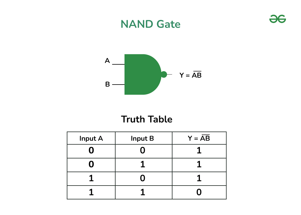
NAND Gate
From the symbol it is clear that it is simply and AND gate with an inversion that means it takes the input and simply do and operation and then invert or complement the result to give the NAND operation result.
Truth Table of NAND Gate
The output of NAND Gate is false only when both input is high otherwise it is true for all other input.
NAND gate can be used in electronic circuits in various devices such as transistors, diodes, or in combination circuit for designing of logic gates.
Implementation Of NOT Gate Using NAND Gate
We know that the NAND gate is a universal gate therefore it is used to implement any basic gate. The implementation of NOT gate using NAND gate is shown

NOT Gate using NAND Gate
It is clear from the above diagram to implement NOT gate using NAND gate we have to join both the input of NAND gate to get a single input of NOT gate and the output of the NOT gate is taken from the output of the NAND gate.
- As we know the output of the NAND gate is (AB)’,So After joining both the input together we get output as (AA)’=A'(Using boolean Algebra).
The above setup complements the input hence implementation of NOT gate is done using NAND gate.
Conclusion
In conclusion, the NOT gate is the basis of digital logic design and has applications in many areas, including arithmetic, storage devices, and control circuits. It is often used in conjunction with other gates to perform complex logic operations. The use of NAND gates provides high performance, capacity and deep understanding of digital content. It demonstrates the powerful performance and versatility of NAND gates in digital electronic devices and provides an electronic design model.
Implementation of NOT Gate using NAND Gate – FAQs
What is the use advantage of NAND gates for logic design?
NAND gates are universal gates so one can implement any basic type of gate using NAND gate. This help in simplified circuit design because you can us it to create all other basic logic gates. This leads to simpler and more efficient designs.
Why use NAND gate to implement NOT gate?
NAND gate are universal gate so you can implement any basic logic gate from NAND gate. So using NAND gate demonstrates this universality.
How do We physically connect NAND gates to create NOT gates?
To create NOT gate using NAND gate simply connect both the input of the NAND gate together. This will result you inverse of the input signal.
Share your thoughts in the comments
Please Login to comment...