IC Fabrication Process
Last Updated :
27 Feb, 2024
In this article , we will discuss about the Integrated Circuits- and its Fabrication Process. Firstly the topic will cover the basic concept of Integrated Circuits , that they are basically the circuit which has large number of resistor , capacitor and transistor which are connected to each other and this all forms a chip . After that we will study in detail about the the fabrication process of Integrated Circuits.
Integrated Circuits
Integrated Circuits (ICs), usually referred to as microchips or chips, are at the middle of modern-day-day digital devices, powering the whole IOT from smartphones and computer systems to clinical tool and vehicle structures. These miniature digital circuits, created from lively and passive components, are fabricated on a silicon substrate.
The integration of numerous additives on an unmarried chip gives several blessings, making ICs a crucial technology within the electronics employer. Here are some of the important factors considered below:

Active and Passive Components in ICs
- Active Components: ICs encompass energetic additives, collectively with diodes and transistors. Diodes are semiconductor devices that permit the go together with the float of electrical present day-day in a single route, allowing capabilities like rectification. Transistors are the building blocks of digital suitable judgment gates and amplifiers, bearing in thoughts sign amplification and switching.
- Passive Components: Passive components in ICs encompass resistors and capacitors. Resistors alter the go along with the float of electrical modern-day-day-day, limiting voltage stages and making sure right sign shaping. Capacitors hold and release electric strength, permitting skills like filtering and power storage.
Why Integrated Circuits?
Integrated Circuits are used for many purposes so the are used such because:
Miniaturization and hence increased equipment density
- One of the most brilliant blessings of ICs is miniaturization. By integrating more than one additives onto a single chip, digital gadgets can end up appreciably smaller and more transportable. This miniaturization allows the introduction of complicated structures in a compact form aspect, predominant to the proliferation of advanced era in our each day lives.
- ICs allow miniaturized digital adders, permitting complex circuits to be positioned in miniature chips. These smaller additives have added on enhancements in small portable digital devices, from smartphones to wearable technology.
Batch Processing and Cost Reduction
- ICs are manufactured the use of batch processing strategies, which notably lessen production expenses. This efficiency stems from the potential to create more than one chips on a single silicon wafer simultaneously. The excessive yield of functional chips in step with wafer reduces the cost in step with unit, making electronics more low cost.
- ICs are synthetic on silicon wafers the use of batch processing strategies. This tool of mass production notably reduces the charge in line with unit. As a give up cease end result, digital communications are in particular less pricey for producers and clients.
Improved System Reliability
- The elimination of soldered joints in ICs enhances tool reliability. Traditional virtual assemblies comprise numerous soldered connections, that may become factors of failure because of thermal pressure and mechanical strain. ICs, with their monolithic introduction, lessen those susceptible hyperlinks and enhance the general reliability of digital structures.
- ICs do away with the want for soldered joints and a couple of discrete connectors that can be reasons of failure in digital systems. This consequences in advanced device-huge reliability due to the fact the capability failure factors are decreased.
Better Functional Performance
- The compact layout of ICs permits for greater inexperienced and optimized circuit layouts. This outcomes in better sensible trendy performance in phrases of tempo, electricity normal performance, and sign excellent. ICs are designed and examined to deliver normal and dependable operation over a massive shape of environmental situations.
- ICs permit more than one digital abilities to be incorporated on a unmarried chip. This integration appreciably improves the overall goal normal overall performance, because of the fact the inclusions can be with out troubles programmed in large numbers on awesome photos.
Matched Devices
- Integrated circuits encompass intently matched additives, making sure ordinary performance and tendencies among diverse chips. This matching is critical in programs like analog signal processing, wherein unique voltage and modern-day tiers have to be maintained for correct operation.
- Transistors and specific energetic connectors on an IC may be matched precisely, making sure that additives with the identical tendencies are used in the equal circuit. This alignment improves the accuracy and balance of the virtual technique.
Increased Operating Speeds and Reduced Power Consumption
- As era advances, ICs maintain to evolve, imparting better working speeds and decreased energy consumption. Advanced production techniques, along with smaller transistor sizes and modern architectures, allow the development of electricity-green and excessive-performance ICs that meet the needs of current packages.
- Adding additives to an unmarried chip reduces the length of communique among them. Small interactions reason fast mark propagation, and vice versa.
Integrated Circuits Fabrication Process
Firstly , fabrication is the process of construction or manufacturing of electronic device or product . Basically it is the process of making large electronic components from may small electronic components .
The process involved for the Integrated Circuits is as follows:
- Silicon Wafer Preparation
- Ion Implantation
- Diffusion
- Photolithography
- Oxidation
- Chemical-Vapor Deposition
- Metallization
- Packaging

IC Fabrication Process
Silicon Wafer Preparation
Silicon Wafer Preparation is the first step of IC Fabrication and usually silicon is used in Integrated Circuits Fabrication Process . Wafer is the base of the Integrated Circuits -which is thin, round shaped with varying diameter . The material used in this making is pure crystalline silicon . Some wafers have irregular – shape, surface , extra edges so in order to make it at a particular thickness the shaping , polishing and cutting is done .
Ion Implantation
Ion Implantation is the process to implant the impurities in the silicon wafer . The ions get penetrated to the wafer which depends on the accelerating field voltage . This process is performed at low temperature so that it can be maintained at room temperature and at high energy , but sometimes the high energy distort the structure of solid . High energy dopant ions are used to penetrate on the surface of the solid and it is the controllable process which is able to change the properties of the solid.
.webp)
Ion Implantation
Diffusion
Diffusion is the process of adding impurities to the silicon from high concentration region to low concentration region. The impurities or we can say the dopants added to the silicon changes the resistivity of the silicon. Dopants used can be of any state- solid , liquid or gas. This process is carried out at high temperature(around 1000 degree Celsius) in furnaces so we can say that it is very much temperature dependent. Pentavalent or n type impurity are preferred as dopants . This process is not performed at last stages because number of layers are formed initially so high temperature it is not able to resist.
Photolithography
Photolithography is the process of producing the film with the help of light , the type of light used is of different frequencies- X ray light , UV light and most probably the UV light is used . The incident of light takes place directly or through the lens. Photoresist is the sensitive material which forms the first layer over the surface of wafer and above the photoresist layer a mask pattern is formed.
The pattern is formed and some are is left exposed and on that exposed area UV light falls and breaks the photoresist layer and soften part of the layer gets removed . Photolithography is very efficient method to form patterns but not on the irregular surface.
Oxidation
Basically , Oxidation is the process of addition of oxygen and in this context the addition of oxygen and silicon forms silicon dioxide which forms in furnaces at higher temperature (around 1000 degree Celsius). Silicon dioxide is hard protective coating that is why it is used . Oxidation is of two types : Dry oxidation and Wet oxidation . Both types are good in its own way .
In dry oxidation no water vapour is used so the produced oxide is good and has less defects . Its rate of oxidation is less than that of wet oxidation , but dry oxidation has good electrical properties . On the other hand , wet oxidation is fast because of presence of water vapour the rate of reaction gets fast. Oxidation process is the important part of the fabrication process of any device or component .
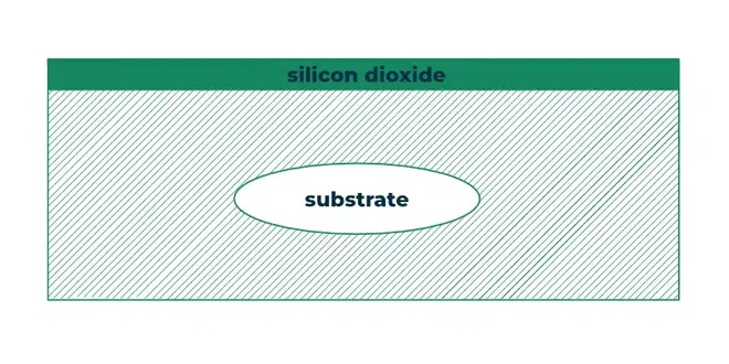
Oxidation
Chemical-Vapor Deposition
CVD method is used in the production of thin films , on the surface of wafer the chemicals and vapours are reacted and form solid , so the layers on the solid get deposited using CVD process. So a high quality solid material is produced and this process is carried out at low pressure , almost lower than the atmospheric pressure and this all depends on the reaction of the process. It is totally different from VCD method . This method has faster deposition rate and acts as an insulator on the surface of wafer.
Metallization
Metallization is the process of coating of metallic layer on the metal and non metallic surface in order to protect the surface from the external environmental factors . This method is also used to connect different components like capacitor , transistor , etc. and the metal layer is form on the wafer then the mask pattern is formed above the layer .It has good conductivity and makes good bond with silicon.
Packaging
Packaging is the last process of IC Fabrication process , in which the silicon wafer is tested electrically that how it is working , either working or not .This method is cost effective because for checking purpose of the wafer , machines includes microwave and radio frequency testing. the circuits which are having any defect are separated from them and the circuits which are proper and good are send for further process or to header .This method also assembles ICs with the other devices and makes a product which can be suitable to use t the end.
The packaging is sealed with plastic so that it can be protected from the external environmental factors and prevent it from oxygen to get inside the packaging so it is performed in the vacuum.
Conclusion
Integrated circuits have revolutionized the electronics corporation through using manner of supplying a compact and charge-effective answer for a huge sort of virtual packages. The integration of lively and passive additives on a single silicon substrate has precipitated smaller, more reliable, and higher-performing digital gadgets, the usage of technological improvements and improvements in present day-day interconnected worldwide. With ongoing research and improvement, included circuits will hold to play a pivotal function in shaping the future of electronics.
Share your thoughts in the comments
Please Login to comment...