The transistor was invented in 1948 by John Bardeen, Walter Brattain, and William Shockley at Bell Laboratory in America. The invention of the transistor completely revolutionized the electronic industry. Since then, there has been a rapidly expanding effort to utilize and develop many types of semiconductor devices such as FET, MOSFET, UTJ, SCR, etc. transistors have replaced bulky vacuum tubes in performing many jobs.
When a third doped element is added to the crystal diode in such a way that two P-N junctions are formed, the resulting device is known as a transistor. The transistor━ an entirely new type of electronic device is capable of achieving amplification of weak signals. As the transistor has two P-N junctions, one junction is forward biased and the other junction is reversed biased. The forward-biased junction has a low resistance path whereas a reverse-biased junction has a high resistance path. The weak signal is introduced in the low-resistance, circuit, and output is taken from the high-resistance circuit.
Transistors can operate in three regions namely cut-off, active, and saturation regions. To operate the transistor in the desired region we have to apply the external DC voltages of correct polarity and magnitude to the two junctions of the transistor.
What is Transistor Biasing ?
Transistor biasing is defined as the proper flow of zero signal collector current and the maintenance of proper collector emitter voltage during the passage of a signal. Transistors can operate in three regions namely cut off, active and saturation region. To operate the transistor in the desired region we have to apply the external dc voltages of correct polarity and magnitude to the two junctions of the transistor. The basic purpose of transistor biasing is to keep the base-emitter junction properly forward biased and collector-base junction reverse biased during the application of signal.
Need for Transistor Biasing
- For proper working it is essential to apply voltages of correct polarity across its two junctions.
- If it is not biased correctly, it would work inefficiently and produce distortion in the output signal.
- Operating point should bot be affected due to temperature changes and device variations.
- Further for various applications , transistor is biased as shown in table.
|
Region of operation
|
Base Emitter Junction
|
Collector Base Junction
|
Application
|
|
Cut off
|
Reverse biased
|
Reverse biased
|
As a switch
|
|
Active
|
Forward biased
|
Reverse biased
|
As an amplifier
|
|
Saturation
|
Forward biased
|
Forward biased
|
As a switch
|
Factors Affecting the Operating Point
The point obtained on the dc load line by the value Ic and VCE when no signal is applied at the input is known as operating point.
The following are the factors that affect the stability of the operating point-
- Temperature dependence of IC .
- Change of VBE and β due to replacement of transistor.
- Thermal runway.
What is Stabilization?
The process of making operating point independent of temperature changes or variations in transistor parameters is known as stabilization. When the temperature changes or when the transistor is replaced by same type, the operating point (i.e., zero signal ICQ and ICEQ ) also changes. For faithful amplification, it is essential that operating point remains fixed. This necessitates to make the operating point independent of these variations. This is known as stabilization.
Need for Stabilization
The need for stabilization lies in various dependencies:
- Temperature Dependence of IC : We know the collector current is given as –
IC=βIB+(1+β) ICBO
where, β= Common emitter current gain
IB = Base current
ICBO= Leakage current.
The above three variables are strongly temperature dependent. Hence, with the increase in temperature, if any of these parameters changes, then collector current changes and so operating point is shifted to any other region.
- Variation in Parameters between Transistors of Same Type : Even after the tremendous advances in semiconductor technology, the transistor parameters such as β vary widely between transistors even of same type. Change in β will shift the operating point in any undesired region.
- Thermal Runway : The collector current is given as
IC= βIB + (1+β) ICBO
If temperature changes then ICBO changes which turn changes IC and operating point. Flow of collector current in the collector circuit produces heat at the collector junction. This raises the temperature. Hence ICBO increases which in turn increases collector junction and the whole process repeats again. Such successive increase in IC, will drive the operating point into saturation region. This process is also called thermal runway. This is a very dangerous situation because due to excessive heat the transistor may burn out.
- Bias Stability : It is necessary that IC should be kept constant in spite of variations of ICBO or ICO. the extent to which a biasing circuit is successful in maintaining this is measured by Bias Stability Factor.
By definition,
S=dIC/dICO : at constant IB and β
Hence we can understand that any change in collector leakage current changes the collector to a great extent. The stability factor should be as low as possible so that the collector current doesn’t get effected.
- Negative Feedback: If the original input signal and feedback signal are out of phase then it is called negative feedback. It is used in amplifiers. We have seen that negative feedback reduces the gain of the amplifiers but still it is employed in almost all the amplifier circuits. It is because the negative feedback improves the overall performance and stability of an amplifier.
Types of Transistor Biasing
The following are the most commonly used types of transistor biasing are as below :
- Fixed bias circuit (Single base resistor biasing) or base bias.
- Collector to base bias circuit.
- Voltage divider bias circuit (V.D.B.) or self bias.
- Emitter bias or modified fixed bias circuit.
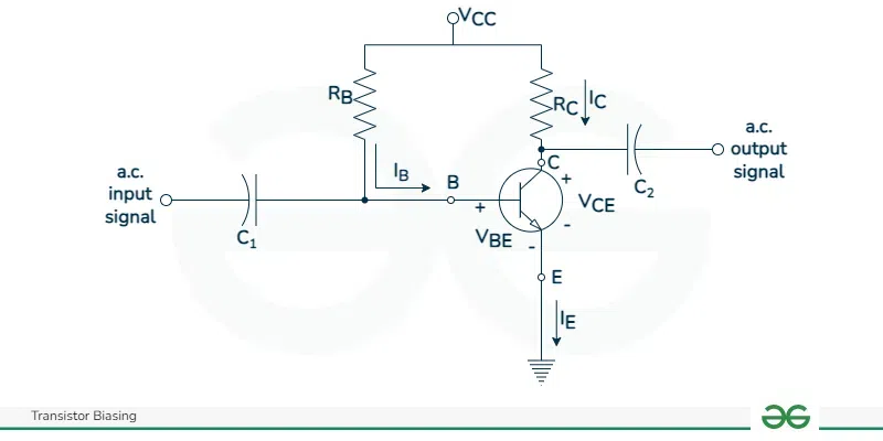
Fixed Bias Circuit
In this, a resistance RB is connected between supply VCC and base terminal of the transistor. The required zero signal base current IB is provided by VCC and a single VCC keeps the base emitter junction forward biased and the collector base junction reverse biased.

Fixed Bias Circuit
Base Circuit (at the input end)
Apply K.V.L. to the base circuit-
VCC-IBRB-VBE=0
IBRB=VCC-VBE
IB=(VCC-VBE)/RB
IB≅ VCC/RB (∵VCC>>VBE)
- For silicon transistors VBE is 0.7 V and for germanium transistors VBE is 0.3 V.
- In this circuit, the supply VCC is of a fixed value. As the resistance RB is selected, IB is also fixed.
Hence this circuit is called as fixed bias circuit.
Collector Circuit (at the output end)
Now apply K.V.L. to the collector circuit.
VCC-ICRC-VCE=0
VCE=VCC-ICRC
ICRC=VCC-VCE
IC=VCC-VCE/RC
The collector current in CE configuration is given as,
IC=βIB+ICEO
where ICEO→ Leakage current
IC=βIB (∵βIB>>ICEO)
Advantages of Fixed Biased Circuit
- It is a simple circuit.
- The operating point can be fixed anywhere in the active region of the characteristics by simply changing the value of RB.
- Biasing conditions are set easily.
- No loading effect as no resistor is present at base-emitter junction.
- Due to their simplicity fixed bias circuits are cost effective.
Disadvantages of Fixed Biased Circuit
- Poor thermal stability.
- Since IC=βIB is already fixed. IC depends on β which is different for same type of transistor and shifts the operating point.
- Adjusting the operating point over a wide range may be challenging with fixed bias, limiting its suitability for certain applications.
- Potential for thermal runaway.
- Limited temperature compensation leads to changes in bias point.
Collector Biased Circuit
In this, one end of RB resistor is connected to the base and the other end to the collector. here, the base current is not determined by VCC.

Collector Biased Circuit
Base Circuit: Apply K.V.L. to it:
VCC=(IC+IB)RC+IBRB+VBE
VCC=ICRC+IBRC+IBRB+VBE
But IC=βIB,
∴ VCC=βIBRC+IBRC+IBRB+VBE
VCC=IB[(1+β)RC+RB]+VBE
∴ IB=(VCC-VBE)/{(1+β)RC+RB
Collector Circuit
Apply K.V.L. to this circuit,
VCC=(IC+IB)RC+VCE
VCC=ICRC+IBRC+VCE
∴ VCE=VCC-(IC+IB)RC
IC=βIB
∴ IC=β[(VCC-VBE)/(1+β)RC+RB
Advantages of Collector to Base Bias Circuit
- It is a simple circuit.
- It provides some stabilization of the operating point.
- It needs only one resistor at base.
- Reduced sensitivity to transistor variations.
- Lower sensitivity to the power supply changes.
Disadvantages of Collector to Base Bias Circuit
- It does not provide good stabilization because stability factor is high.
- It provides a negative feedback which reduce the gain of the amplifier.
- Dependency on component matching.
- More complex in comparison to fixed bias circuits.
- Restricted utilization in certain application with specific voltage requirements.
Voltage Divider Bias Circuit
The voltage divider is formed by R1 and R2. The voltage drop across R2 forward biases the base emitter junction. The R1 and R2 resistor act as a voltage divider giving a fixed voltage at point B which is base. This is the most widely used biasing method that provides biasing and stabilization to a transistor.

Voltage Divider Bias Circuit
Base Circuit: Voltage across R2 is the base voltage VB.
Apply voltage divider to this circuit
∴ VB=(VCCR2)/(R1+R2)
Collector Circuit: Voltage across RE is VE and can be obtained as
VE=IERE=VB-VBE
IE=(VB-VBE)/(RE)
Apply K.V.L.
VCC=ICRC+VCE+VE
VCE=VCC-ICRC-IERE
Advantages of Voltage Divider Base Circuit
- IC in this circuit is almost independent of transistor parameters.
- The resistor employed in the emitter provides stabilization.
- It is the most prominent one.
- Flexibility in adjusting operating point.
- Moderate sensitivity to power supply changes.
Disadvantages of Voltage Divider Base Circuit
- The signals tend to get mixed up.
- It requires more components.
- Due to the increased complexity, it tend to be more expensive.
- It can lead to reduction in overall circuit efficiency due to the power dissipation.
- Dependency on component matching.
Modified Fixed Bias Circuit (Fixed Bias With Emitter Resistor)
In this, resistor RE has been added from emitter to the ground terminal of the fixed bias circuit. This is done to improve the stability of the circuit.

Modified Fixed Bias Circuit
Base Circuit
Apply K.V.L. to this circuit
VCC=IBRB+VBE+IERE
But IE=IB+IC
and IC=βIB
On substituting the value of IC in IE, we get
IE=IB+βIB
Now substituting the value of IE in VCC
VCC=IBRB+VBE+(βIB+IB)RE
=IB(RB+βRE+RE)+VBE
∴ IB=(VCC-VBE)/(RB+βRE+RE)
Collector Circuit
Apply K.V.L. to this circuit,
VCC=ICRC+VCE+IERE=ICRC+VCE+(IB+IC)RE
VCE=VCC-IBRE-IC(RC+RE)
IC=βIB
∴ IC=β[(VCC-VBE)/(RB+βRE+RE)]
Advantages of Modified Fixed Bias Circuit
- The addition of emitter resistor provides improved stability.
- It provides a high voltage gain.
- It is a simple circuit, with enhanced stabilization.
- Reduced sensitivity to transistor variations.
- It can strike a balance between simplicity and performance.
Disadvantages of Modified Fixed Bias Circuit
- Its operating point can be effected by change in temperature.
- It requires the use of dual polarity power supply.
- Limited voltage range.
- Potential for component matching.
- Complex circuit.
Solved Example on Transistor Biasing
1. For the fixed bias circuit determine IB, IC, VCE, VB, VC and VBC for the following parameters RB = 240 KΩ , RC= 2.2 KΩ , VCC= 12 V and β=50.
As it is fixed bias circuit
We have IB = (VCC – VBE)/ RB
∴ IB= (12-0.7)/ 240 KΩ = 47.08μA
∵IC= β IB
∴ IC= 50 x 47.08μA = 2.35mA
∵VCE = VCC– ICRC
∴VCE = 12 – 2.35mA x 2.2 KΩ= 6.83 V
∵Emitter terminal is grounded
∴ VB= VBE= 0.7V
VC = VCE= 6.83 V
∵VBC= VB– VC
∴VBC= 0.7V – 6.83V = 6.13 V
Transistor Biasing
Biasing in Amplifier Circuits
In all amplifier circuit, the DC bias is provided by the voltage divider circuit of resistances R1 and R2 and emitter resistor RE provides stabilization. the value of R1 and R2 are such that the current through them is 10 times the base current (IB) and the value of RE is in between 500 and 1000 Ω.

Common Emitter Amplifier
Applications of Transistor Biasing
|
Type
|
Parameter Analysis
|
Application
|
|
Fixed Bias Circuit
|
β dependent, unstable Q point
|
Digital Switch
|
|
Collector To Base Bias
|
Greater stability
|
Amplifier
|
|
Voltage Divider Bias Circuit
|
β independent, stable Q point
|
Amplifier
|
|
Emitter Bias Circuit
|
Greater stability
|
Ic driver amplifier
|
Conclusion
Transistors are one of the most widely used semiconductor devices which are used for a wide variety of applications, including amplification and switching. However, to achieve these functions satisfactorily, a transistor must be supplied with a certain amount of current and/or voltage. Biasing is necessary to keep the transistor in its active region, where it can amplify signals without distortion. A Stability factor is a measure of the stability of a transistor amplifier circuit with respect to changes in transistor parameters like input and output current and voltages due to temperature, aging, or other factors.
FAQs on Transistor Biasing
What is meant by transistor biasing ?
Transistor biasing is defined as the proper flow of zero signal collector current and the maintenance of proper collector emitter voltage during the passage of a signal.
Why is transistor biasing necessary?
- For proper working it is essential to apply voltages of correct polarity across its two junctions.
- If it is not biased correctly, it would work inefficiently and produce distortion in the output signal.
- Operating point should bot be affected due to temperature changes and device variations.
What are the different types of transistor biasing?
- Fixed bias circuit (Single base resistor biasing) or base bias.
- Collector to base bias circuit.
- Voltage divider bias circuit (V.D.B.) or self bias.
- Emitter bias or modified fixed bias circuit.
Share your thoughts in the comments
Please Login to comment...