As we all know, based on conductivity, we divide the material into three categories: Conductor, Semiconductor, and Insulator. In which the conductivity of the conductor is highest, insulators have the lowest conductivity, and semiconductors have intermediate conductivity. The reason behind this is the number of free electrons present in the crystal of each material. If we talk about the conductivity of semiconductors, two different types of semiconductors are classified based on the number of electrons and holes present in the crystal: Intrinsic and Extrinsic semiconductors. In this article, we will discuss these semiconductors, especially extrinsic semiconductors, their properties, formation, needs, and various applications.
What are Semiconductors?
It is defined as the material that shows both the properties of the conductor and the insulator in different conditions. The conductivity of a semiconductor lies between the conductor and the insulator. Some examples of elementary semiconductors are silicon (Si) and germanium (Ge).
Energy Band Theory
Based on Pauli’s exclusion principle, the energy of an electron is definite in a single isolated atom, but after the formation of a molecule or crystal, the energy of an electron is not fixed but varies in some range, which is called the energy band. There are two important bands: The valence band and the Conduction band, respectively.
- Valence band: It represents the energy of bonded electrons, which are present in the valence band and do not take part in conduction.
- Conduction band: It represents the energy of free electrons, which are present in the conduction band and take part in conduction.
- Forbidden energy gap: It is defined as the energy gap between the valence and conduction band, and it is known as forbidden because no electron is present inside this energy gap. It is represented as ΔEg.
Classification of solids based on energy band theory:
-(2)-(1)-660.png)
Classification of solids based on energy band theory
Effect of Temperature on Semiconductor
- Case 1: When the temperature is equal to 0k.
At T = 0k, all the valence electrons are bound in the valence band, and no electron is free to move in the crystal, as a result of which the semiconductor behaves as a perfect insulator.
- Case 2: When the temperature is greater than 0k.
At T > 0k, due to thermal energy some covalent bonds break and electrons are free to move in the crystal, leaving behind a vacancy called a hole. Due to the generation of electron-hole pair in the crystal, the semiconductor behaves as a conductor.
Properties of Semiconductors
- There are two charge carriers present in the semiconductors, i.e. an electron and a hole.
- The hole is considered the imaginary charge carrier in the semiconductor.
- Electrons and holes both have the same magnitude of charge but opposite signs.
- The mobility of a hole is less than the mobility of an electron.
- The net current of the semiconductor is due to the movement of electrons and holes, i.e Itotal = Ie + Ih
- The net conductivity of a semiconductor is also due to both charge carriers, i.e σtotal = σe + σh
Types of Semiconductors
Based on the number of electrons and holes, there are two types of semiconductors: Instrinc and Extrinsic
Intrinsic semiconductor
A semiconductor in which the number of electrons is equal to the number of holes is known as an intrinsic semiconductor. It is also known as a pure semiconductor because there exists no impurity that has been added to this semiconductor.
Condition for intrinsic / Pure semiconductor: ne = nh = ni
where ne = number of electrons
nh = number of holes
ni = intrinsic carrier concentration
As the number of electrons and holes are equal in the intrinsic semiconductor, it is electrically neutral.
At room temperature, the conductivity of intrinsic semiconductors is very low, and it is not fit for designing any practical devices.
What is Doping?
As we discussed, the conductivity of intrinsic semiconductors is very low, so to increase the conductivity of the semiconductor we add some impurity atoms to the semiconductor, which are known as dopants, and the process is known as doping.
Conditions for doping:
- The doping ratio must be equal to 1 ppm (1 part per million), that means for every 106 pure atoms there exists 1 impure atom, i.e. 106: 1
- The size of a dopant / impure atom must be equal to the size of a pure atom, to maintain the crystal structure.
b) Extrinsic Semiconductor
A semiconductor in which the number of electrons and holes are unequal is known as an extrinsic semiconductor. An extrinsic semiconductor is formed by adding the impure atom or dopant to the pure semiconductor. It is also known as an impure and doped semiconductor.
Extrinsic / Impure / Doped semiconductor = Instrinsic / Pure semiconductor + Dopants
In extrinsic semiconductors, doping is done to increase the conductivity of semiconductors, so we can use them to create some practical devices. If we consider Silicon or Germanium as our semiconductor, there are two different groups of elements that are suitable for use as dopants, Group 13 (BORON FAMILY) & Group 15 ( NITROGEN FAMILY) based on the conditions of doping.
Types of Extrinsic Semiconductor:
Depending on the type of dopants we use, there are two different types of extrinsic semiconductors formed:
- N-type extrinsic semiconductor
- P-type extrinsic semiconductor
N-type semiconductor
It is formed when pentavalent impurities were added to the semiconductor. It is also known as donor impurity.
When any dopant atom is added to a semiconductor crystal, like silicon, it replaces the silicon atom and makes a bond with another silicon atom, when we add a pentavalent impurity, five out of four electrons are only able to make the bond with their neighboring silicon atom, but that one extra electron is not able to make any bond, and it freely moves in the entire semiconductor crystal. As a result of which, the conductivity of semiconductors increases. As we see by adding a pentavalent impurity to the semiconductor, it donates an electron in the crystal, and that is why it is also known as a donor impurity atom.
Examples of pentavalent dopant atoms are Phosphorus, Arsenic Antimony, etc.
In N type semiconductor, the majority charge carriers are electrons and minority charge carriers are holes.
Condition in N type semiconductor : Ne >>> Nh
Therefore the current in N type semiconductor is due to electrons only, Itotal ≅ Ie.
And the conductivity is also due to electrons only σtotal ≅ σe
Ne ≅ ND where ND is Donar atom density
The block diagram of an N-type semiconductor:
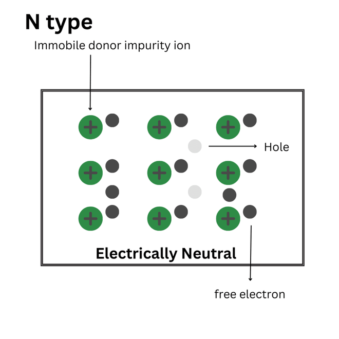
Block diagram of an N-type Semiconductor
The energy level diagram of an N-type semiconductor:
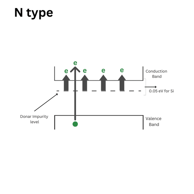
The energy level diagram of an N-type semiconductor
b) P-type semiconductor
It is formed when trivalent impurities(Boron family) were added to the semiconductor. It is also known as acceptor impurity. When any dopant atom is added to a semiconductor crystal, like silicon, it replaces the silicon atom and makes a bond with another silicon atom, and when we add a trivalent impurity, all three electrons make bonds with the neighboring silicon atom and a vacancy is created in the semiconductor crystal known as a hole. All the neighboring electrons try to fill this vacancy, resulting in a creation of a new vacancy at their site. This is how the movement of the hole takes place. As a result of which, the conductivity of semiconductors increases. As we see by adding a trivalent impurity to the semiconductor, it accepts an electron from the crystal, and that is why it is also known as an acceptor impurity atom.
Examples of trivalent dopant atoms are Boron, Aluminium, Indium, etc.
In P type semiconductor, the majority charge carriers are holes and minority charge carriers are electrons.
Condition in P type semiconductor : Nh >>> Ne
Therefore the current in P type semiconductor is due to holes only, Itotal ≅ Ih.
And the conductivity is also due to holes only σtotal ≅ σh
Nh ≅ NA where NA is Acceptor atom density
The block diagram of a P-type semiconductor:

Block diagram of a P-type semiconductor
The energy level diagram of a P-type semiconductor:
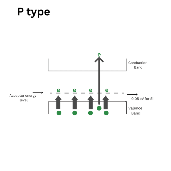
The energy level diagram of a P-type semiconductor
Conclusion
In this article, we learn that a semiconductor is a type of material that shows both the property of conductors and insulators, its classification is based on energy band theory and different properties like having two different charge carriers: electron and hole respectively. Then we classify semiconductors into two different types: intrinsic and extrinsic, based on the number of electrons and holes present in the crystal. Due to the low conductivity of intrinsic semiconductors, we made extrinsic semiconductors by adding some impure atoms in them, to increase their conductivity, and this leads to the formation of two different types of extrinsic semiconductors: N and P-type semiconductors. In N-type semiconductors, the majority charge carriers are: electrons and minority charge carriers are: holes. On the other hand in P-type semiconductors, the majority of charge carriers are: holes and the minority of charge carriers are: electrons. Extrinsic semiconductors are used in various practical devices such as P-N Diode, ICs, Solar cells, sensors, and in detectors.
FAQs on What is Extrinsic Semiconductor?
Q.1: Does extrinsic semiconductors are electrically neutral?
Answer:
Yes, extrinsic semiconductors are electrically neutral, although the number of electrons and holes are unequal the electrical neutrality is maintained in both the N and P type of semiconductor.
Q.2: What is Mass-Action law?
Answer:
It defines the relationship between ne, nh, and ni . According to mass action law, At thermal equilibrium, the product of the concentration of electrons and holes is equal to the square of intrinsic concentration.
Q.3: Do holes moves in a crystal?
Answer:
In actual, electrons are moving in order to fill the vacancy (holes) in the crystal, leaving behind a vacant at their lattice site, but it appears that holes are moving, which is not the real case.
Q.4: List some applications of extrinsic semiconductors.
Answer:
Due to high conductivity and application in making of practical devices, extrinsic semiconductor are used in various applications like:
- P-N Diodes
- Integrated Circuits
- LEDs
- Electronic Detectros
- Sensor
Share your thoughts in the comments
Please Login to comment...