Binary Adder with Logic Gates
Last Updated :
26 Apr, 2024
Binary Adder and logic gates are important elements in digital logic. Binary adders are circuit which adds two binary numbers and results in the sum of the two binary numbers. Logic gates are the circuit in which a signal can pass through if a logic is applied through it. In this article we will discuss about the binary adder with logic gates, binary adder, logic gates and implementation of binary adder with logic gates. We will also discuss the required formulas and solve some examples related to the binary adder. Let’s start our learning on the topic “Binary adder with logic gates.”
What is Logic Gate?
A logic gate is a circuit in which when a logic is applied a signal can pass through it. There are seven commonly used logic gates namely, AND gate, OR gate, NOT gate, NAND gate, NOR gate, XOR gate, and XNOR gate. These logic gates help in the implementation of different circuits. The logic gates are the fundamental building blocks of a digital circuit. Logic gates are used Mostly in digital circuit design to perform various logical operations, enabling the creation of complex digital systems. By combining these basic gates in different configurations, We can design circuits that perform a wide range of functions, from simple arithmetic to complex data processing.
What is Binary Adder?
A binary adder is a circuit used to add two binary numbers. It takes two binary numbers as input and gives sum of the two binary numbers and their carry as output. ALU uses a binary adder for addition. Binary Adders can be implemented using various Configuration,But most of the common Configuration is Using Half Adder and Full Adder Circuit.A half adder adds two single-digit binary numbers and produces the sum and carry output. However, a full adder extends this functionality to accommodate an additional carry input from the previous bit position, allowing it to add three input bits (two operands and the carry from the previous addition) to produce the sum and carry output.
The implementation of binary adder can be done with the help of half adders and full adders. Below we will discuss half adders, full adders and implementation of binary adder using half and full adders.
What is Half Adder ?
Half adder is a combinational circuit that is used to add two 1-bit inputs to generate sum and carry as outputs. The expression for sum and carry in the half adder is given by XORing both the inputs and by product of both the inputs respectively.
Let A and B be two 1-bit inputs then,
Expression for Sum S
Sum= A ⊕ B
Where,
A,B are the Inputs
Expression for Carry
Carry = A.B
Where,
A,B are the Inputs

Half Adder
Block Diagram and Logic Diagram for Half Adder
Below is the block diagram and logic diagram for the half adder.

Block Diagram of Half Adder
What is a Full Adder ?
Full adder is a combinational circuit used to add three 1-bit inputs and generates sum and carry as outputs. The expression for the sum and carry in full adder is given by XORing all the three inputs and by product of sum of all three inputs respectively.
Let A, B and C are three 1-bit inputs,
Expression for Sum
Sum = A ⊕ B ⊕ C
Where,
A,B,C are the Inputs
Expression for Carry
Carry = AB + BC + AC
A,B,C are the Inputs

Full Adder
Block Diagram and Logic Diagram for Full Adder
Below is the block diagram for full adder

Block diagram of Full Adder
Implementation of Binary Adder with Logic Gates
For the implementation of binary adder, we use full adders and half adder.
- First, we take two n-bit binary numbers as input.
- The full adders can add only three 1-bit numbers so, we take the first bit of one number and corresponding first bit of second number and the past generated carry as the input to the full adder.
- The above process is repeated for all the n-bits of the inputs.
- We will connect multiple full adders to add two n-bit binary numbers.
- If we have n-bit inputs then, we connect n-full adders.
- The sum output of each full adder is arranged accordingly to get the sum of the two n-bit binary numbers.
- The carry output of the full adders is given as input to the next connected full adder. The carry output of last full adder gives the carry generated or provides the information about the Overflow condition.
- So, by implementing the above we get binary adder with logic gates (present in full adders).
Logic Diagram for Binary Adder using Full Adder
Let A and B are two 4-bit binary numbers and S represents the n-bit sum of these two inputs. Below is the logic diagram for the binary adder.
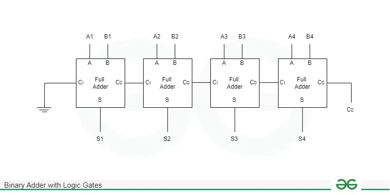
Binary Adder
Note: In the above diagram instead of first full adder we can use half adder as Ci for first adder is grounded.
Required Formulas in Binary Adder
The full adders have propagation delays for sum and carry generation. The time required by the full adder to generate sum is called sum propagation delay and the time required by the full adder to generate carry is called the carry propagation delay.
The formula for the sum propagation delay of full adder is given by:
Sum Propagation Delay = Propagation delay of XOR gate
The formula for the carry propagation delay of full adder is given by:
Carry Propagation Delay = Propagation delay of AND gate + Propagation delay of OR gate
We know that the binary adder is implemented by cascading the full adders hence it requires time to produce sum and carry output. So, the formula for the time required to generate carry and sum bit of ith full adder is given below.
The formula to calculate the time required to get the carry bit of the ith full adder is:
Time required to get the carry bit of the ith full adder = Number of full adders before ith full adder × Carry propagation delay of full adder
The formula to calculate the time required to get the sum bit of the ith full adder is:
Time required to get the sum bit of the ith full adder = (Number of full adders before ith full adder × Carry propagation delay of full adder) + Sum propagation delay of full adder
Solved Examples
Find the time required to get sum bit of third full adder of the binary adder. Given that the carry propagation delay and sum propagation delay of the full adder is 5 ns and 8 ns respectively.
Solution:
We know that,
Time required to get the sum bit of the ith full adder = (Number of full adders before ith full adder × Carry propagation delay of full adder) + Sum propagation delay of full adder
Time required to get the sum bit of the third full adder(S3) = [(3 – 1) × 5] + 8
S3 = 10 + 8
S3 = 18 ns
Find the time required to get carry bit of fifth full adder of the binary adder. Given that the carry propagation delay of the full adder is 9 ns.
Solution:
We know that,
Time required to get the carry bit of the ith full adder = Number of full adders before ith full adder × Carry propagation delay of full adder
Time required to get the carry bit of the 5th full adder (C5) = 5 × 9
C5 = 45 ns
Advantages and Disadvantages of Binary Adder
Some advantages and disadvantages of the binary adder are given below:
Advantages of Binary Adder
Some advantages of the binary adder are:
- Using binary adders n-bits inputs can be added easily.
- All the n-bits of the two binary numbers can be provided to the adder simultaneously.
Disadvantages of Binary Adder
Some disadvantages of the binary adder are:
- The circuit becomes complex.
- The past carry bits are required as input.
- It has some propagation delay.
Applications of Binary Adder
Some applications of the binary adder are listed below:
- Binary adders are used for addition in ALU.
- Binary adders are used in the digital gadgets to perform arithmetic operations.
- Microcontrollers use the binary adders for the increment purposes.
Conclusion
From the above discussion we can conclude that the binary adder can be implemented using the full adders and half adder. As the full adders and half adders are the combinational circuits made up of logic gates hence, the binary adder is implemented using the logic gates. If the two binary numbers are of n-bits then we require either n full adders or (n – 1) full adders and 1 half adder. So, by cascading the full adders we can implement the binary adder.
Binary Adder with Logic Gates – FAQs
How Do You Make Binary Adders Using Logic Gates?
Binary adders using logic gates can be made by full adders and half adder.
What Gates are Involved in the Binary Adder?
The logic gates XOR, OR and AND gates are involved in the full adders and half adders and the binary adder is implemented using the half and full adders. So, the gates involved in the binary adder are XOR gate, OR gate and AND gate.
What is 4-Bit Binary Adder?
The binary adder used to perform addition of 4-bit binary numbers is called 4-bit binary adder.
Share your thoughts in the comments
Please Login to comment...