CPU control design and Interfaces
Question 1
Consider the following statements.
- I. Daisy chaining is used to assign priorities in attending interrupts.
- II. When a device raises a vectored interrupt, the CPU does polling to identify the source of interrupt.
- III. In polling,the CPU periodically checks the status bits to know if any device needs its attention.
- IV. During DMA, both the CPU and DMA controller can be bus masters at the same time.
Question 2
Consider the following data path diagram.
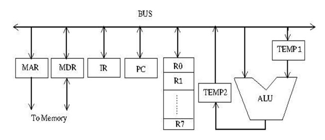 Consider an instruction:
Consider an instruction:
R0 ← R1 + R2The following steps are used to execute it over the given data path. Assume that PC is incremented appropriately. The subscripts r and w indicate read and write operations, respectively.
- R2r, TEMP1r, ALUadd, TEMP2w
- R1r, TEMP1w
- PCr, MARw, MEMr
- TEMP2r, R0w
- MDRr, IRw
Question 4
Consider the following sequence of micro-operations.
     MBR ← PC
     MAR ← X
     PC ← Y
     Memory ← MBR
Which one of the following is a possible operation performed by this sequence?
Question 5
The use of multiple register windows with overlap causes a reduction in the number of memory accesses for
I. Function locals and parameters
II. Register saves and restores
III. Instruction fetches
Question 6
Consider a main memory system that consists of 8 memory modules attached to the system bus, which is one word wide. When a write request is made, the bus is occupied for 100 nanoseconds (ns) by the data, address, and control signals. During the same 100 ns, and for 500 ns thereafter, the addressed memory module executes one cycle accepting and storing the data. The (internal) operation of different memory modules may overlap in time, but only one request can be on the bus at any time. The maximum number of stores (of one word each) that can be initiated in 1 millisecond is ____________
Question 7
Which one of the following is true for a CPU having a single interrupt request line and a single interrupt grant line?
Question 8
Consider the following data path of a simple non-pilelined CPU. The registers A, B, A1, A2, MDR, the bus and the ALU are 8-bit wide. SP and MAR are 16-bit registers. The MUX is of size 8 × (2:1) and the DEMUX is of size 8 × (1:2). Each memory operation takes 2 CPU clock cycles and uses MAR (Memory Address Register) and MDR (Memory Date Register). SP can be decremented locally.
The CPU instruction “push r”, where = A or B, has the specification
M [SP] ← r
SP ← SP – 1
How many CPU clock cycles are needed to execute the “push r” instruction?
Question 9
What is the minimum size of ROM required to store the complete truth table of an 8-bit x 8-bit multiplier?
Question 10
A CPU has only three instructions I1, I2 and I3, which use the following signals in time steps T1-T5:
I1 : T1 : Ain, Bout, Cin
T2 : PCout, Bin
T3 : Zout, Ain
T4 : Bin, Cout
T5 : End
I2 : T1 : Cin, Bout, Din
T2 : Aout, Bin
T3 : Zout, Ain
T4 : Bin, Cout
T5 : End
I3 : T1 : Din, Aout
T2 : Ain, Bout
T3 : Zout, Ain
T4 : Dout, Ain
T5 : End
Which of the following logic functions will generate the hardwired control for the signal Ain ?
There are 39 questions to complete.
Last Updated :
Take a part in the ongoing discussion