- Interview Prep
- Tutorials
- Tracks
GATE EC || ELECTRONIC DEVICES AND CIRCUIT || SEMICONDUCTORS || PYQS (2000-2025)
Question 1
As shown, a uniformly doped Silicon (Si) bar of length
L = 0.1μm with a donor concentration ND =1016 cm-3 is illuminated at x =0 such that electron and hole pairs are generated at the rate of
GL = GL0 1-xL,0≤x≤L,
where GL0 = 1017 cm–3 s–1. Hole lifetime is 10–4s, electronic charge q = 1.6 × 10⁻¹⁹C, hole diffusion coefficient Dp = 100 cm2/s and low-level injection condition prevails. Assuming a linearly decaying steady state excess hole concentration that goes to 0 at x = L, the magnitude of the diffusion current density at x = L/2, in A/cm2, is ____.
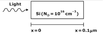
( GATE 2017 || EC || NAT ||1 MARK)
16
Question 2
In a non-degenerate bulk semiconductor with electron density n=1016cm−3, the value of EC−EFn=200meV, where EC and EFn denote the bottom of the conduction band energy and electron Fermi level energy, respectively. Assume thermal voltage as 26 meV and the intrinsic carrier concentration is 10cm−3. For n=0.5×1016cm−3, the closest approximation of the value of (EC−EFn), among the given options, is ______.
(GATE 2022 || EC || MCQ ||1 MARK)
226 meV
174 meV
218 meV
182 meV
Question 3
Select the CORRECT statement(s) regarding semiconductor devices.
(GATE 2022 || EC || MSQ ||1 MARK)
Electrons and holes are of equal density in an intrinsic semiconductor at equilibrium
Collector region is generally more heavily doped than Base region in a BJT.
Total current is spatially constant in a two terminal electronic device in dark under steady state condition
Mobility of electrons always increases with temperature in Silicon beyond 300 K.
Question 4
For an intrinsic semiconductor at temperature T=0 KT=0 K, which of the following statement is true?
All energy states in the valence band are filled with electrons and all energy states in the conduction band are empty of electrons.
All energy states in the valence band are empty of electrons and all energy states in the conduction band are filled with electrons.
All energy states in the valence and conduction band are filled with holes.
All energy states in the valence and conduction band are filled with electrons.
Question 5
For an intrinsic semiconductor at temperature T=0 KT=0 K, which of the following statement is true?
(GATE 2023 || EC || MCQ ||2 MARK)
All energy states in the valence band are filled with electrons and all energy states in the conduction band are empty of electrons.
All energy states in the valence band are empty of electrons and all energy states in the conduction band are filled with electrons.
All energy states in the valence and conduction band are filled with holes.
All energy states in the valence and conduction band are filled with electrons.
Question 6
The free electron concentration profile n(x)n(x) in a doped semiconductor at equilibrium is shown in the figure, where the points A,BA,B, and CC mark three different positions. Which of the following statements is/are true?
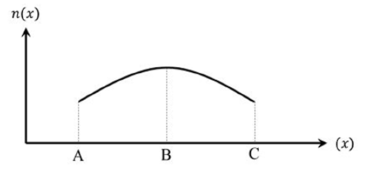
( GATE 2024 || EC || MCQ ||2 MARK)
For xx between B and C, the electron diffusion current is directed from C to B.
For xx between B and A, the electron drift current is directed from B to A.
For xx between B and C, the electric field is directed from B to C.
For xx between B and A. the electric field is directed from A to B.
Question 7
Consider a MOS capacitor made with p-type silicon. It has an oxide thickness of 100 nm, a fixed positive oxide charge of 10−8C/cm2 at the oxide-silicon interface, and a metal work function of 4.6eV. Assume that the relative permittivity of the oxide is 4 and the absolute permittivity of free space is 8.85×10⁻¹⁴ F/cm. If the flatband voltage is 0 V0 V, the work function of the pp-type silicon (in eV, rounded off to two decimal places) is _
(GATE 2024 || EC || MCQ ||2 MARK)
4.32
Question 8
A non-degenerate n-type semiconductor has 5\% neutral dopant atoms. Its Fermi level is located at 0.25eV0.25eV below the conduction band (EC) and the donor energy level (ED) has a degeneracy of 2. Assuming the thermal voltage to be 20mV20mV. The difference between EC and ED (in eV, rounded off to two decimal places) is
( GATE 2024 || EC || NAT ||2 MARK)
0.18
Question 9
The intrinsic carrier concentration of a semiconductor is 2.5×10¹⁶/m32.5×1016/m3 at 300 K.
If the electron and hole mobilities are 0.15 m2/Vs and 0.05 m2/Vs, respectively, then the intrinsic resistivity of the semiconductor (in kΩ.m ) at 300 K is __________ .
(Charge of an electron e=1.6×10⁻¹⁹C
(GATE 2025 || EC || MCQ ||1 MARK)
1.65
1.25
0.85
1.95
Question 10
The electron mobility μn in a non-degenerate germanium semiconductor at 300 K is 0.38 m2/Vs.
The electron diffusivity Dn at 300 K (in cm2/s, rounded off to the nearest integer) is __________ .
(Consider the Boltzmann constant kB=1.38×10⁻²³ J/K and the charge of an electron e=1.6×10⁻¹⁹C)
(GATE 2025 || EC || MCQ ||1 MARK)
26
98
38
10
There are 29 questions to complete.