Flash-Based solid-state drive (SSD)
Last Updated :
28 Nov, 2022
As introduced in this article, solid-state storage devices (SSDs) do not contain any moving parts. They are rather made of transistors, and can retain information in case of power loss, unlike random-access memory. Flash is an interesting technology developed in the 1980s. Storing Bits: Flash chips can store one or more than one bits in a single transistory. The amount of charge trapped in the transistor is converted to a binary number. Depending on the number of bits stored in a single transistor, flash chips can be of various types:
- Single-Level Cell (SLC) Flash: Only a single bit is stored in a transistor. The bit value can therefore be 0 or 1.
- Multi-Level Cell (MLC) Flash: Two bits are stored in a transistor. The bit value can therefore be 00, 01, 10 and 11 – from the lowest to the highest charge levels.
- Triple-Level Cell (SLC) Flash: Three bits are stored in a transistor.
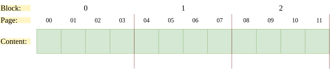
SLC chips have the highest performance and are most expensive of the three. Banks and Planes: Storing a single bit is, obviously, not enough. Therefore, flash chips are grouped into banks or planes which are made up of a large number of cells. Banks: Banks are organized into blocks and pages. Blocks range from the size 128-256 KB and pages are about 4 KB. The figure below shows a sample flash chip, containing 3 blocks and 4 pages per block, i.e. a total of 3*4 = 12 pages.
The blocks and pages structure is extremely crucial for flash operations. Flash Operations: Below are the three low-level operations supported by flash operations.
- Read: To read a page, the flash client simply needs to specify the page number issued with the read command. Random access devices allow any information to be read uniformly and quickly, irrespective of its location.
- Erase: Before one can write to a page in flash, it is necessary that the corresponding entire block be erased. To erase a block, the value of each bit is set to 1. Since the data must get written again, it is copied to a buffer before the erase command.
- Program: After erasing a block, the program command changes some of the 1’s to 0’s.
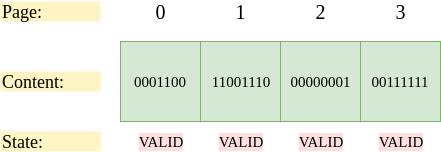
Reading a page is the fastest command and takes an order of 10 microseconds to complete. Programming a page is the second fastest, taking an order of 100 microseconds. Erasing a block is the slowest because the contents need to copied to a buffer before the block is emptied out, and takes a few milliseconds to complete. States of Pages: Flash pages have “states” associated to them. Initially, all pages are in the INVALID state. If a block is erased, all pages within that block change to the ERASED state. Such pages are programmable since they can accept writes. When a page is programmed, it changes to the VALID state. This means the contents of the page can be read. Consider the following initial orientation of a block containing 4 pages. Since each of these pages has been programmed before and have some already existing data written onto them, they are all in the VALID state.
Now, assume the flash client wishes to write to page 0. To write to any page, the entire block needs to be erased.
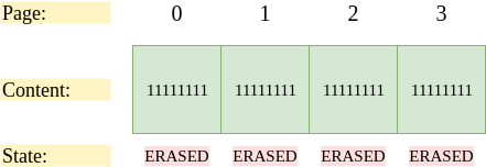
After erasing the entire block, all 4 pages are in the ERASED state and all bits are set to 1. Finally, we can write to page 0.
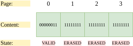
Page 0 is now in the VALID state since the new data has been written onto it and it can be read from. The other pages are still in the ERASED state. Finally, the data previously stored in pages 1, 2 and 3 are read from the temporary memory and written back into the pages. Reliability Issues: Frequent writes and erases lead to wear out of the flash chips. This happens because of the excess charge accumulated onto the surface of the flash block. As more and more charge accrues, it becomes difficult to differentiate between a 0 and a 1. The block then becomes unusable and needs to be discarded. The second reliability issue is disturbance. This happens because of the flipping of bits in neighbouring pages when trying to read/write data on a particular page. These are also called read disturbs or program disturbs. Flash-Based SSDs: Flash-based SSDs provide an interface on top of the flash chips to read/write data. An SSD contains flash chips for persistent memory; non-persistent memory e.g. SRAM used for caching and buffering; and control logic to handle the flash operations. Flash Translation Layer (FTL) converts client read and write requests into flash operations, which are low-level operations. It essentially converts logical operations to physical operations with high reliability. FTL also helps counter some of the reliability issues mentioned above.
- Handling wear outs: FTL spreads out and uniformly distributes the flash blocks as much as possible, such that all the blocks wear out around the same time.
- Handling disturbance: To handle disturbance while programming the chips, FTL takes up a sequential programming approach. Erased blocks are programmed in order, from lowest to the highest page, thereby overwriting any bits flipped in the process.
Log-Structured FTL: Similar to the log-structured file systems, most FTLs today are log-structured, meaning writes are grouped together in a buffer before being physically executed onto the flash blocks.
Like Article
Suggest improvement
Share your thoughts in the comments
Please Login to comment...