Counter-Type Analog-to-Digital Converter (ADC)
Last Updated :
29 Apr, 2022
Analog-to-Digital Converters (ADC) are typically used in all modern-day systems. The main job of the ADC is to convert the analog signal to a digital binary signal. Why digital signal? The reason is that digital data is easy to process, store and transmit. With advancements in CMOS technology, it has been possible to fabricate thousands of logic circuits and gates on a 1mmx1mm chip. Digital binary data, represented by low and high voltage levels at the hardware level, can be used for all kinds of arithmetic operations, using combinatorial circuits, and storage, using sequential circuits. The transmission of digital data lowers the chances of communication errors. This necessitates the need for several types of ADCs, each having some pros and each being a right fit for a particular application.
There are many ADCs: slope-type, counter-type, tracking-type, and flash ADCs. Here we are going to discuss the counter-type ADC.
Counter-Type ADC
The counter-type Analog-to-Digital Converter (ADC) is also known as the digital ramp ADC. It is because the output of the counter is fed to a Digital-to-Analog Converter (DAC), and while the counter increments its count, the output of the DAC increases in ramp fashion or staircase fashion.
The counter-type ADC uses a counter for conversion from analog to digital.
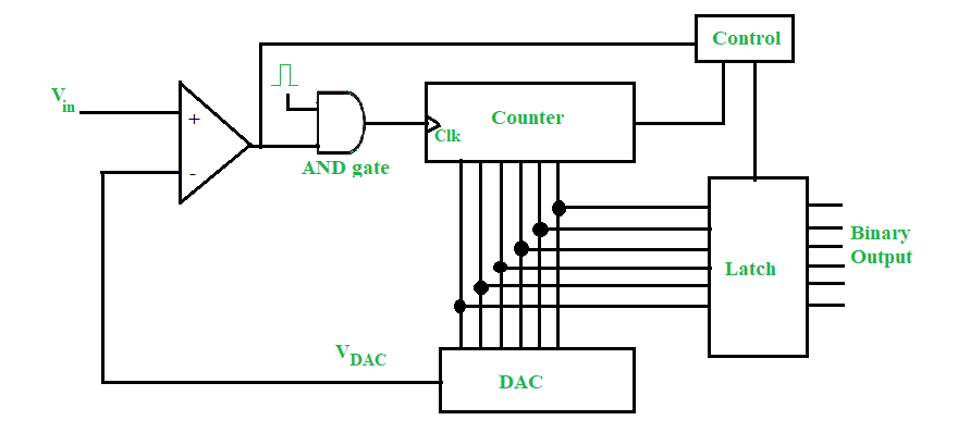
Counter-type ADC
Counter-Type ADC Operation
During the start of the conversion, the output of DAC is zero. So, whatever input voltage Vin is applied at the positive terminal of the comparator, the output of the comparator is high. Since it is high, the AND gate is enabled and it allows the clock pulse to pass. The counter then starts counting the clock pulses. The output of the counter is fed to the DAC, which computes the decimal equivalent of its binary input. Now, the output of the DAC VDAC increases in a staircase fashion and it is continuously compared with the input Vin. As long as Vin > VDAC, the counter keeps counting.
The moment Vin < VDAC, the comparator output is low, and AND gate is disabled, therefore blocking the clock pulses. Also, the control block notices this transition and puts a low signal in the clear pin of the counter, thereby resetting it. Simultaneously, the last output of the counter is latched and this is the digital binary output of the given input voltage.
So, the basic principle of operation of the counter-type ADC is to keep counting the number of clock pulses till the input is greater than the DAC output and the moment DAC output is greater than the input, the counter is reset and the last count is latched and given as output.
Counter-type ADC Conversion Time
Conversion time for any ADC is defined as the time taken by it to convert a given analog input to a digital binary output. It is analogous to the propagation delay we study in digital logic gates.
If the counter has to count from the zeroth state (that is all 0s) and counts up to N, then the conversion time is (N-1)Tc, where Tc is the time period of the clock pulse. Maximum conversion time occurs when the input voltage is equal to the full-scale output range of the DAC. The DAC gives a full-scale output when all bits are one. To reach all ones from all zeroes, the counter takes 2n-1 clock pulses, where n is the number of bits. Hence, maximum conversion time = (2n-1)Tc.
Advantages
The counter-type ADC is simple and easy to use. It is very accurate and the precision can be increased by increasing the number of bits. While there are many complicated ADCs in the market, counter-type ADC has a fair balance of accurate output and cheap hardware costs.
Disadvantages
The major drawback of this ADC is that every time a new conversion starts, the counter is reset and it has to start counting right from all zeroes. Hence, the conversion time is significant. It cannot sustain high-frequency input, as it will not be able to convert the analog signal to digital binary in real-time. The worst case occurs when the input voltage is equal to the full-scale output range of the DAC.
Like Article
Suggest improvement
Share your thoughts in the comments
Please Login to comment...