For computers, it is as difficult to understand words and numbers as humans can, computers need a specific language to understand it. To make the complicated data understood by computers, binary coding is used. In binary, data is represented with the combination of two digits, either 0 or 1.
To store the data effectively, binary registers are used in computers. The binary registers refer to a method, which is used to store the data in computers. where flip-flop, as a one memory cell, is used to store digital data. It is a useful method to increase the capacity of data storage, which works in terms of bits.
Here, in this article, we are going to discuss the importance of binary registers in the process of storing data, it’s working, and the structure of registers.
The Binary Cell
The binary cells are kind of storage cells that are capable of storing one binary digit or binary character. They are used to store information in digital electronics.
When a cell is read, it saves one bit of binary data, and before it can be accessed, it must be set to store a 1 and then reset to a 0.
The block diagram for a Binary cell, along with the circuit symbol is below:
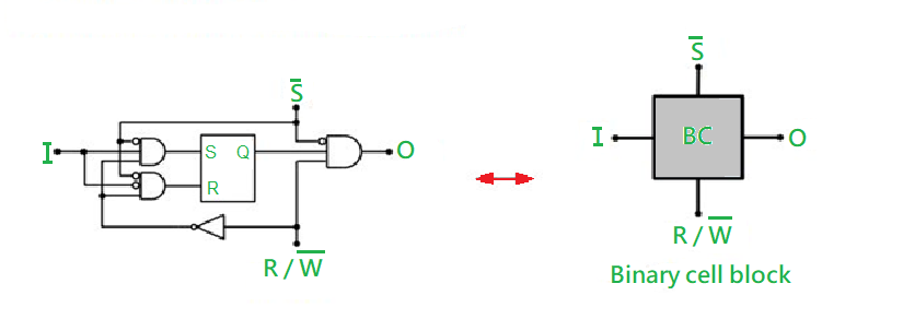
Binary Cell
Binary Registers
Binary registers are referred to as the effective method to store digital data. Binary registers use flip-flops, as a memory cell, to store the data. It is a good way of storing data, which works in terms of bits. Here, a group of flip-flops is used to store the data, which are usually called registers.
As an example, in the n-bit register, there will be n number of flip-flops. And it will be capable of storing the n-bit word.
Binary Register Data
The binary registers are used to measure the outcomes of a qubit, which are usually called Declared states. Declared states are always represented in 0 or 1. Often they are referred to as the measurement registers.
While creating a qubit register, using qubits instruction, the binary-registers can be created with the same number of entries. For instance, qubits 5 creates a qubit register for 5 qubits, along with that, a binary register with 5 entries.
In the binary register, entries can be used to control quantum algorithms, by using controlled gates. the index, which is been used to address the qubit register and the binary, both are similar
The other thing is that, in the binary registry, number 1 will be shown as 01, Similarly, the number 10 will be represented as 0A.
A Register is a kind of circuit made up of Flip-Flops that can store data in a form of one bit. a register is a sequential logic circuit in digital electronics.
The Structure of Registers
The registers are a group of flip-flops and gates, the flip-flops are responsible for the binary information, and on the other hand, the gates are the controllers, which are responsible to decide when and how the new information is transferred into the registers.
There is various type of registers are available, but talking about the simplest one, the register, which consists of only flip-flops and no external gates are less complicated.
While understanding the structure of registers, here are some of the elements, that we need to know, are given below:
The Loading Registers: The transfer of new data into a register is called a loading register. And if all register bits are simultaneously loaded with the regular clock pulse, then it is called to be done in the parallel state.
Register Transfer Language
The Register transfer language is initially a symbolic language that describes a micro-operation transfer between registers.
The term register transfer refers to the usability of hardware logic circuits, which can transfer the result of the operation to the same or another register, by performing the state micro-operation.
In other words, this kind of programming language is a method of expressing a computer process through symbols.
Here are some commonly used registers, which are given below:
1. The Accumulator: These registers are the most common type of registers. Which is used to store data measured from memory.
2. The General-Purpose Registers: During program execution, this type of register is used to store data intermediate results. It can be accessed by assembly programming.
3. The Special Purpose Registers: These registers are used by the Computer system only. For example, some of the names are given below:
- PC: The Program Counter indicates the next instruction to be executed.
- IR: The instruction to be executed is stored in the Instruction Register or IR.
- MBR: Memory Buffer Registers, It stores instructions and data transferred to and received from the memory.
- MAR: MAR stands for Memory Address Register, which are registers that holds the address for the memory unit.
The Register Transfer
The register transfer refers to the way hardware logic circuits perform a micro-operation to transfer the data from one register to another, which is presented in a specific symbolic form. To understand it better, you can look at the statement below;
Mainly, the registers that are used for specific operations are listed down:
- PC: The Program Counter indicates the next instruction to be executed.
- IR: The instruction to be executed is stored in the Instruction Register or IR.
- MAR: MAR stands for Memory Address Register, which are registers that holds the address for the memory unit.
- R1: The Processor Register. There are some Individual bits, which also be indicated by putting them in parenthesis. For instance, PC (8-15), R2 (5), and so on.
Replacement Operation: Data transfer from one register to another is represented symbolically by the replacement operator. For example, the following statement represents a data transfer from register R1 to register R2.
Statement: R2 ← R1
Usually, we intend to transfer only in the conditions, where the control conditions are predetermined. This statement can be understood by looking at the following:
Statement: if (P=1) then (R2 ← R1)
Here, P is referred to as a control signal, which is generated through a control section.
Here you can take a look at the image showing the block diagram that depicts the transfer of data from R1 to R2.
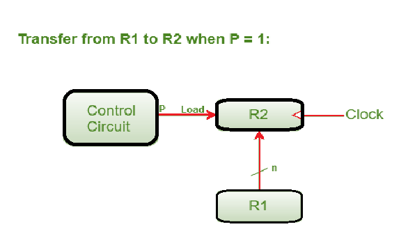
Data transfer from R1 to R2
Here, in the diagram, the letter ‘n’ stands for the number of bits in the register. The register R1’s ‘n’ outputs are linked to the register R2’s ‘n’ inputs.
The control variable ‘P’ activates a load input, which is then transmitted to the register R2.
How information is transferred among Registers?
The binary data in a register can be shifted from one flip-flop to another within the register. The registers, which allow this kind of transfer is called Shift registers. In the shift register, there are four modes of operation, which makes it easy to transfer data.
To understand it briefly, the list is down below:
- Serial Input Serial Output
- Serial Input Parallel Output
- Parallel Input Serial Output
- Parallel Input Parallel Output
1. Serial Input Serial Output:
- The Serial Input Serial Output keeps the flip-flops in the reset condition. Like Q3 = Q2 = Q1 = Q0 = 0.
- If an entry of a four-bit binary number 1 1 1 1 is applied in the register, this number should be applied to Din
- bit with the LSB bit applied first. The input D of FF-3.
- Here, D3 is connected to serial data input Din. The output of FF-3 i.e.
- And, Q3 is connected to the next input flip-flop i.e. D2 and so on.
To understand it clearly, you can see in the diagram below:
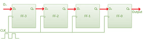
Block diagram of The Serial Input Serial Output
2. The Serial Input Parallel Output:
- Here in this type of operation, the data is entered serially and exited in parallel form.
- Data is loaded one bit at a time. While the data is loaded, the outputs are disabled.
- Once the data loading is complete and all of the flip-flops have their required data, the outputs are activated so that all of the loaded data is available on all of the output lines at the same time.
- A four-bit word requires four clock cycles to load. As a result, the SIPO mode operates at the same speed as the SISO mode.
For better understanding, you can see the diagram below:
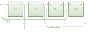
The block diagram of The Serial Input Parallel Output
3. Parallel Input Serial Output (PISO):
- Data bits are entered in parallel.
- The following circuit is a four-bit parallel input serial output register.
- A combinational circuit connects the output of the previous Flip Flop to the input of the following one.
- The binary input words B0, B1, B2, and B3 are all fed into the same combinational circuit.
- This circuit can operate in one of two modes: shift mode or load mode.
Load Mode: When the shift/load bar line is low (0), the AND gates 2, 4, and 6 become active and pass the bits B1, B2, and B3 to the respective flip-flops. The binary inputs B0, B1, B2, and B3 will be loaded into the respective flip-flops on the low going edge of the clock. As a result, parallel loading occurs.
Shift Mode: When the shift/load bar line is low (1), the AND gates 2, 4, and 6 are turned off. As a result, concurrent data loading is no longer possible. However, AND gates 1, 3, and 5 become active. As a result, when clock pulses are applied, data is shifted from left to right bit by bit. As a result, the parallel in serial out operation occurs.
Here you can see the block diagram down:
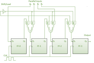
The block diagram of The Parallel Input Serial Output (PISO)
4. Parallel Input Parallel Output (PIPO):
In this kind of mode operation, the four-bit binary inputs B0, B1, B2, B3 are applied to the four flip-flops’ data inputs D0, D1, D2, D3. And when a negative clock edge is applied, the input binary bits are simultaneously loaded into the flip-flops. The loaded bits will appear on the output side at the same time. Only a clock pulse is required to load all of the bits.
Here is the block diagram below to understand it better:
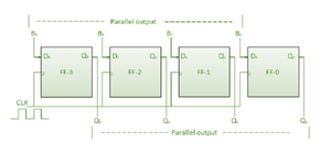
The block diagram of The Parallel Input Parallel Output (PIPO)
Here, we have talked about binary Data registers and how it works. Overall, we can say that binary data registers are a beneficial method for storing binary data in a faster and more efficient manner. Data can be transported and stored in a flexible manner using binary data registers.
Like Article
Suggest improvement
Share your thoughts in the comments
Please Login to comment...