1 Bit Full Adder using Multiplexer
Last Updated :
10 Sep, 2021
Prerequisite : Multiplexer, Full adder
Introduction :
Multiplexer and Full adder are two different Digital Logic circuits. The Multiplexer is a digital switch. It allows digital information from several sources to be routed onto a single output line. On the other hand, the Full adder circuit performs the addition of three bits and produces the Sum and Carry as an output. Our aim is to build the Full Adder circuit using Multiplexers rather than the usual basic logic gates.
Step 1 – To implement a full adder using MUX, we need to first create the truth table of the full adder.
- Truth Table for Full Adder –
| Inputs |
Outputs |
| A |
B |
C-In |
Sum |
C-Out |
| 0 |
0 |
0 |
0 |
0 |
| 0 |
0 |
1 |
1 |
0 |
| 0 |
1 |
0 |
1 |
0 |
| 0 |
1 |
1 |
0 |
1 |
| 1 |
0 |
0 |
1 |
0 |
| 1 |
0 |
1 |
0 |
1 |
| 1 |
1 |
0 |
0 |
1 |
| 1 |
1 |
1 |
1 |
1 |
Step 2 – We need to find out the minterms for the Sum and Carry output from the truth table.
For Sum -     f ( A, B, C-In) = Σ ( 1,2,4,7 )
For Carry: -  f ( A, B, C-In) = Σ ( 3,5,6,7 )
Step 3 – Now we need the equations for Sum and Carry. To find that we will create the Design Table for Sum and Carry output.
NOTE : To understand the next parts it is recommended to go through with Implementation of SOP function using multiplexer
Design Table for Sum Output :
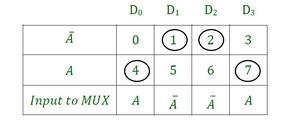
Design Table for Sum
For Sum the minterms (1,2,4,7 ), outputs are HIGH so they are circled in the design table.
- For D0 only 4 is HIGH which corresponds to A in table, So the D0 input for the MUX(M0) will be A.
- The same rule follows for the other inputs – D1=A’, D2=A’, D3=A.
Design Table for Carry Output :
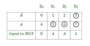
Design Table for Carry
For Carry ( 3, 5, 6, 7 ), outputs are HIGH, so they are circled in the design table, just like the design table for sum.
- Here for the D0 input 0 and 4, both are LOW, so input to the MUX will be 0
- For D3 both 3 and 7 are HIGH, so the input to MUX will be 1.
- D1 and D2 will follow the previous rule and will be D1=A and D2=A
Now we have all the input information to the MUX, so we can design the logic circuit.
Logic Circuit :

Explanation :
Inputs –
The input to the M0 MUX is as per the design table of SUM i.e. D0 = A, D1 = A’, D2 = A’, D3 = A
The input to the M1 MUX is as per the design table of CARRY i.e. D0 = 0, D1 = A, D2 = A, D3 = 1
The selection line of both M0 and M1 are connected with the B & Cin input.
Outputs –
The output of M0 MUX will have the SUM as output and M1 MUX will have CARRY as output.
Applications:
This circuit is a Full adder circuit, so will have all the applications that of a full adder circuit. Lists below –
- The basic building block of on-chip libraries.
- In processors and other kinds of computing devices adders are used in the arithmetic logic unit.
Like Article
Suggest improvement
Share your thoughts in the comments
Please Login to comment...